

The SiD Digital ECal Based on Monolithic Active Pixel Sensors
by
 ,
,
James E. Brau
1,*,
Martin Breidenbach
2,
Alexandre Habib
2,
Lorenzo Rota
2 and
Caterina Vernieri
2 1
Department of Physics, University of Oregon, Eugene, OR 97403, USA
2
SLAC National Accelerator Laboratory, 2575 Sand Hill Road, Menlo Park, CA 94025, USA
*
Author to whom correspondence should be addressed.
Instruments 2022, 6(4), 51; https://doi.org/10.3390/instruments6040051
Submission received: 11 August 2022
/
Revised: 8 September 2022
/
Accepted: 10 September 2022
/
Published: 23 September 2022
(This article belongs to the Special Issue Selected Papers from the 19th International Conference on Calorimetry in Particle Physics (CALOR 2022))
Abstract
:The SiD detector concept capitalizes on high granularity in its tracker and calorimeter to achieve the momentum resolution and particle flow calorimetry physics goals in a compact design. The collaboration has had a long interest in the potential for improved granularity in both the tracker and ECal with an application of monolithic active pixel sensors (MAPS) and a study of MAPS in the SiD ECal was described in the ILC TDR. Work is progressing on the MAPS application in an upgraded SiD design with a prototyping design effort for a common SiD tracker/ECal design based on stitched reticules to achieve 10 × 10 cm2 sensors with 25 × 100 micron2 pixels. Application of large area MAPS in these systems would limit delicate and expensive bump-bonding, provide possibilities for better timing, and should be significantly cheaper than the TDR concept due to being a more conventional CMOS foundry process. The small pixels significantly improve shower separation. Recent simulation studies confirm previous performance projections, indicating electromagnetic energy resolution based on digital hit cluster counting provides better performance than the SiD TDR analog design based on 13 mm2 pixels. Furthermore, the two shower separation is excellent down to the millimeter scale. Geant4 simulation results demonstrate these expectations.
1. Introduction
The physics goals of future electron–positron colliders motivate measurements of unprecedented precision. These will improve understanding of the Higgs boson and top quark, and enable searches for new phenomena that might discover beyond the standard model electroweak particles. With the consequential challenging demands for tracking, heavy-quark tagging, jet energy measurement, and beam polarization measurement, for example, advances in silicon detectors bear significant potential impact. Hadronic jet measurements by particle flow analysis (PFA), based on the combination of a precision tracker and a highly granular calorimeter, will be improved with new low-mass and highly granular sensors. To achieve these goals, several hundred square meters of silicon sensors are needed for low-mass trackers and sampling calorimetry, as envisioned in the SiD design of the ILC Technical Design Report (TDR) [1]. Trackers will require nearly one hundred square meters from the multiple layers at large radii, with micron-scale resolution. Sampling calorimeters need an order of magnitude larger areas of thinned overall packages for reduced Moliere radius, providing excellent shower containment. Silicon monolithic active pixel sensors (MAPS) present an attractive approach to this application.
2. Large-Area MAPS for Future Linear e+ e− Collider
MAPS devices, with silicon diodes and readout circuitry contained in the same die, can be fabricated in standard CMOS processes, and were identified as a promising technology for high-granularity, low-material budget detectors many years ago [2,3,4,5]. They have several advantages over traditional hybrid pixel detector technologies. They can be built inexpensively, thinned to needs, offer individual pixel readout, are reasonably radiation-hard, and low in mass, while operating at high speeds and low power consumption from a single low-voltage supply. The close connection between a sensor and front-end amplifier, without externally added interconnections, significantly reduces the input capacitance, reducing the noise floor. Operation with smaller signals from thinner sensors is possible with satisfactorily high S/N.
Interconnects, routinely realized with some type of metal spheres or pillars bump-bonding, are on one hand comparative in size with the most recently desired pixel sizes O (10 μm). On the other hand, they are responsible for the dominating contribution to the capacitance seen at the input node of an in-pixel amplifier, effectively dominating otherwise very small sensor capacitance. A reduction in capacitance, owing to low-temperature direct bonding technology, was shown in comparative studies [6] to significantly improve pixel detector performance.
Magnitude, speed and efficiency of collecting charge carriers liberated in interactions of radiation with a sensor can be completely controlled in hybrid pixel detectors. MAPS are dependent on the active sensor volume and possible depletion of the substrate in the CMOS process. To retain the advantage of using standard CMOS processes for building MAPS, the older-generation MAPS, such as those used in the Heavy Flavor Tracker (HFT) at STAR [7], were built in the commonly used low-resistivity (about 10 cm) epitaxial wafer fabrication processes. At that time, thermal diffusion charge collection allowed signal magnitudes on the order of 1 k e−, shared among the neighboring pixels and collected in times on the order of 100 ns [8]. The use of only one type of transistor in pixel circuitry was a significant limitation of the early MAPS. Radiation hardness was on the order 1013 of 1 MeV neutrons equivalent per cm2 and 10 Mrads of the Total Ionizing Dose [9]. These parameters were suitable for the HFT at STAR, the first practical use of MAPS. MAPS simultaneously developed using processes suitable for high-voltage applications have not been used in any experiment yet.
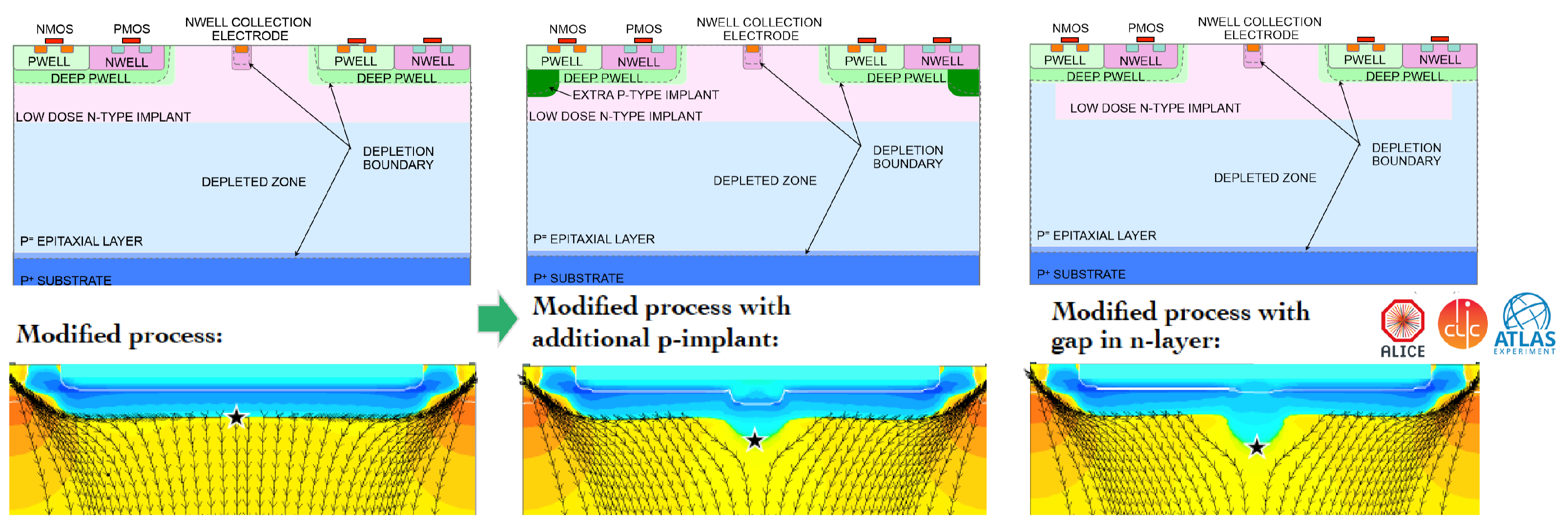
It was shown many years ago that full depletion of the Active Sensitive Volume (ASV) of a device is required for charge to be collected by drift, enabling fast response and radiation hardness. Additionally, both N- and P-type transistors are required in a pixel area to develop efficient processing blocks. As a result of these requirements, new inner trackers, such as the ITS1/2 for ALICE, have employed the increased resistivity of ASV. Figure 1 shows cross-sections of structures built in the TowerSemi aka Tower-Jazz 180 nm. The implantations and distributions of resulting electric fields were optimized [10,11]. A reasonably thick, higher resistivity silicon film, translates to the maximally depleted ASV. Shielding of wells, visible in Figure 1, allows the pixel electronics to employ more than one type of transistor. The key benefit of this in tracking or vertexing, is the increased spatial resolution. While the TowerSemi 180 nm process has been available for the MAPS design for a while, the TowerSemi 65 nm process recently opened up, allowing its exploration to address needs for future applications. The TowerSemi 65 nm process allows a more than four-fold increase in the number of transistors per pixel compared to the 180 nm process. A new generation of MAPS, thinned and on an increased-resistivity substrate (>1 k cm) has been enabled by the developments for ITS3 of the ALICE experiment [12,13,14].
Another key feature of MAPS is the limited chip dimensions of a reticle. The standard 65 nm process limits single chips to about cm2 in process nodes, and even smaller dimensions in earlier processes. This limitation can be overcome by stitching of reticles, or partially by butting [15,16]. While stitching has been available for sometime in commercial CMOS applications, it is less common in particle detector applications; a demonstration has been achieved for X-ray detection [17]. An example of butting is the STAR Heavy Flavor Tracker at BNL RHIC [18], where chips were butted one next to another on the staves and the readout areas of the individual MAPS units were limited to one edge. On the other hand, a few years after the HFT at RHIC, the upgrade of the ALICE Inner Tracker System 3 (ITS3) at the LHC is going to adopt the stitched arrangement of the MAPS devices [12]. Both developments are aimed at targeting inner tracking or vertexing layers for Nuclear Physics experiments, where requirements on readout speed and radiation hardness are less stringent than for many high-energy physics experiments.
At CERN, the ALICE ITS3 upgrade based on MAPS is driving the CERN WP1.2 collaboration investigating wafer-scale MAPS devices on the TowerSemi 65 nm process. Within this collaboration, SLAC is investigating the challenges of wafer-scale designs optimized for detectors at linear machines, focusing in particular on tracking and calorimetry. This effort will help identify the risks that wafer-scale MAPS pose at the system level, such as yield, power distribution and fill factor, as well as evaluate essential aspects of the integration of such devices into a detector system: i.e., cooling, assembly procedures, wafer thinning and handling, and power delivery.
SLAC is developing a readout circuitry optimized for low duty cycle linear collider with bunch spacing as low as a few ns. The beam time structure of these machines (with bunch trains separated by tens-to-hundreds of milliseconds) makes this possible. Two techniques are being implemented. The readout electronics will adopt a power pulsing scheme: the analog front-end circuitry will be powered off during the dead-time between bunch trains. With low duty cycle machines such as ILC and C3 [19], this technique enables a power reduction by more than two orders of magnitude. Power pulsing techniques were previously developed and characterised with the KPiX ASIC [20]. Second, the pixel front-end circuitry will be based on a synchronous readout architecture, where the operation of the circuitry is timed with the accelerator bunch train. In this way, the noise and timing performance of the circuitry can be optimized while maintaining low-power consumption. SLAC will leverage a decade of expertise via synchronous readout architectures operating with fast integration times [21], which have been implemented in all ASICs developed for the Linear Coherent Light Source (LCLS).
By combining all these techniques, the goal of the current R&D at SLAC is to achieve the specifications described in Table 1. We have derived the initial specifications from the C3 configuration, as it bears the most challenging requirements for timing resolution and is compatible with the current limits of MAPS technology. Moreover, a sparse read-out mechanism, based on asynchronous read-out logic, will minimise the digital power as well as render the circuitry more robust to local variations of transistor performance. A first, small-scale prototype of such a device is expected in late 2022.
The development of wafer-scale MAPS will allow designers to investigate the following challenges:
- Power pulsing: Current drawn from the supply needs to reach the peak value in the shortest time possible to take full advantage of the power pulsing technique. This minimizes the duty cycle and thus decreases the average power consumption. However, the instantaneous current consumption of the pixel matrix can reach several Amperes over a few microseconds.
- Power distribution: Distribution of the power supply over a large area is challenging because of the non-negligible voltage drop over long metal distribution lines.
- Yield: Since the probability of fabrication defects scales with the area of the device, it is essential to develop new techniques to mitigate the effects of fabrication defects, such as shorts between supply and ground lines. A defect on one reticle-size MAPS would result in a lower number of usable dies per wafer and a defect on a wafer-scale device is almost inevitable, possibly resulting in the loss of a full wafer.
- Stitching techniques: Design of stitching MAPS introduces additional layout design rules and methodologies, with the goal to increase the fabrication yield. This additional set of rules is not traditionally encountered by ASIC designers. Exposing ASIC designers to such design rules is an essential first step towards the development of wafer-scale devices.
- Assembly and power delivery: Preliminary mechanical and assembly tests need to be conducted to evaluate sensor-power delivery techniques, while minimizing detector dead material.
With the successful resolution of the challenges described here and the development of the MAPS with the target specifications shown in Table 1, they will be applied to the upgrade of the SiD design.
3. SiD
SiD (Figure 2) has been designed to make precision measurements of the Higgs boson, W- and Z-boson, the top quark and other particles at the linear collider. With relatively benign linear collider experimental conditions, the detector can be optimized for these precision measurements. There are lower collision rates, lower complexity, and less background than experienced in a hadron collider.
The requirements in calorimetry performance are driven by excellent jet reconstruction and measurement. Detection and separation of W and Z bosons in their hadronic decay modes is essential, and this motivates application of a PFA and a goal of 3–4% jet mass resolution at energies above 100 GeV, about twice as good as achieved in hadron collisions at the LHC.
In addition, tracking requirements include precise reconstruction of the Z-boson mass in the Higgs recoil analysis, as well as separation of jet flavors for Higgs couplings measurement. The asymptotic momentum resolution requirement for high-momentum tracks is nearly an order of magnitude better than achieved at the LHC, with minimization of detector material to maintain excellent momentum resolution for lower-momentum tracks.
The combination of excellent jet mass resolution, extremely precise tracking, and triggerless running gives SiD at the ILC superb potential for discovery. Quantitatively, the requirements are the following:
- Impact parameter resolution:, where p is particle momentum and is the angle between the particle and the beamline.
- Momentum resolution: asymptotically at high momenta, maintaining excellent tracking efficiency and very good momentum resolution at lower momenta with an aggressive minimization of detector material budget.
- Jet energy resolution:– for light flavour jets with E ≳ 100 GeV based on a PFA; this requires good longitudinal and transverse segmentation, with a minimal Moliere radius.
- Readout: Triggerless.
- Powering: Power of major systems cycled between bunch trains to minimizing cooling requirements and level of inactive material within detector.
The upgrade to MAPS for SiD’s ECal and tracking sensors requires 1364 m2 of silicon, including 54 m2 in the barrel tracker, 20 m2 in the end cap tracker, 1000 m2 in the barrel ECal, and 290 m2 in the end cap ECal. The readout for each bunch train will include a very small fraction of the 540 billion 25 × 100 m2 pixels of the system.
It has been shown that requiring a hit-time resolution below 5 ns for the vertex and tracking detectors, and 1 ns resolution for calorimeter hits, all the particle flow objects have sub-ns time resolution [22]. This is achieved from a truncated mean in the energy-weighted hit times of a cluster; therefore, we expect the ∼ns timing of a large number of MAPS hits to result in a particle flow object time resolution substantially below a nanosecond.
4. MAPS Performance for ECal
The finely granular, digital readout of the SiD ECal offered by application of MAPS sensors provides the potential for significantly enhanced performance over that envisioned in the ILC TDR [1]. One advantage of this digital approach over the TDR analog approach is the reduction in effects due to variations in energy deposition, such as Landau fluctuations. Fluctuations in the development of the shower remain as the main contribution to resolution. The fine granularity also reduces the likelihood of overlapping particles per pixel and improves the separation of nearby distinct showers, such as from high-energy s or jets, and contributes to improved particle flow pattern recognition. Quantifying the nature of these effects has been investigated with Geant4 simulations.
The longitudinal structure of the SiD ECal defined in the ILC TDR remains unchanged in this digital approach. The ECal has thirty total layers. The first twenty layers each have 2.5 mm tungsten thickness and 1.25 mm readout gap. The last ten layers each have 5 mm tungsten plus the same 1.25 mm readout gap. The total depth is 26 radiation lengths, providing reasonable containment for high-energy showers.
The 25 m × 100 m pixel geometry of the 2500 m2 area is chosen for the tracking precision from the 25 m size in the bend plane. Excellent performance with a purely digital ECal based on this fine granularity is expected. A 25 m × 100 m pixel geometry is found to achieve ECal performance equivalent to 50 m × 50 m. Previous studies [23,24,25] have even indicated potential energy resolution advantages for a digital ECal solution and were cited in the ILC TDR. A recent prototype beam test of a similar concept has been published [26].
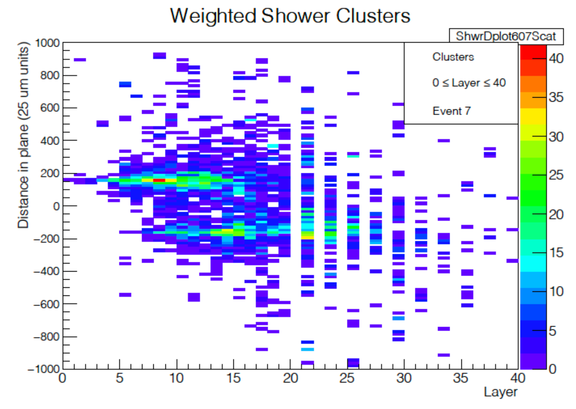
New simulation studies, based on this fine digital configuration, have confirmed the previous studies referred to in the ILC TDR and demonstrated additional details on the performance. These studies indicate the electromagnetic energy resolution based on counting clusters of hits in the MAPS sensors, and weighting them based on longitudinal and transverse position in shower, should provide better performance than the SiD original design based on 13 2 analog pixels, as shown in Figure 3.
Geant4 simulations of the digital MAPS performance applied in the electromagnetic calorimeter have been under development and study since early 2021, and are continuing. These studies are aimed at understanding the ultimate performance and limitations, and to inform the ASIC designers on the requirements for the sensor chips. The expected performance has been found to exceed the requirements and performance of the SiD TDR ECal design. The 5 Tesla magnetic field was found to have a minor effect, degrading the resolution by a few per cent due to the field’s impact on the lower energy electrons and positrons in a shower.
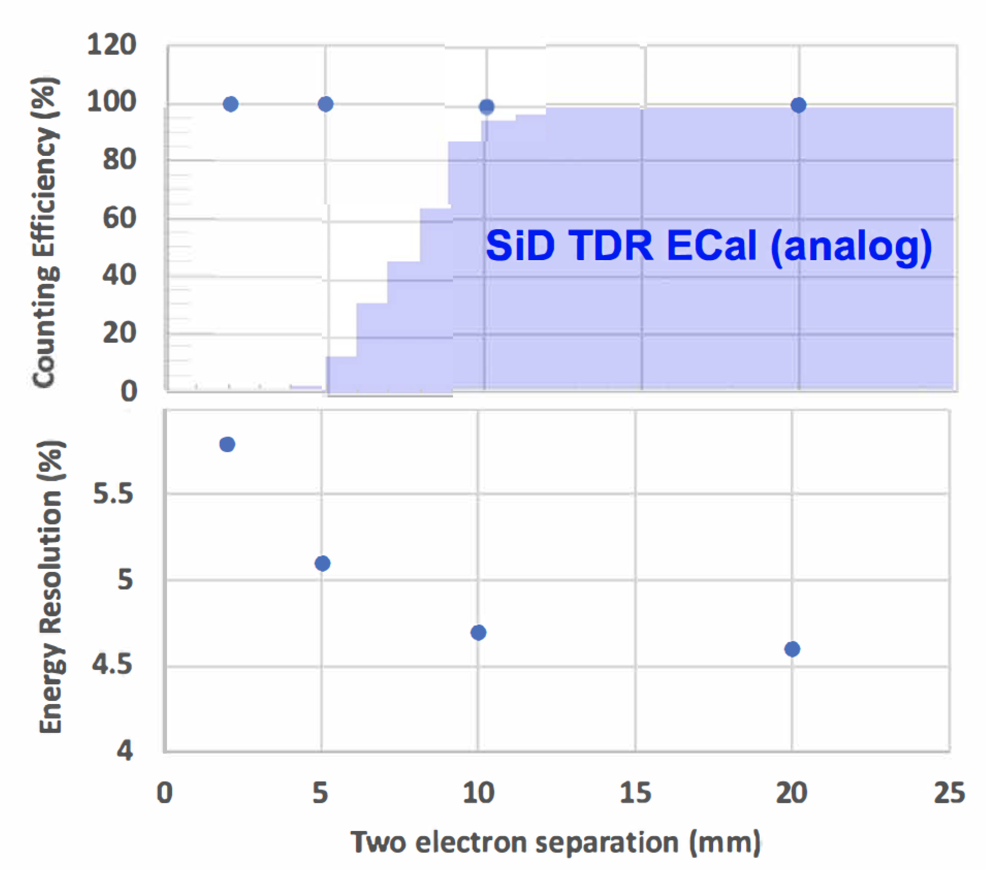
Separation of the two showers is excellent, as shown in Figure 4 for two 10 GeV electron showers separated by one cm and Figure 5 of two 20 GeV gamma showers from a 40 GeV decay. The fine granularity of pixels provides excellent separation. The performance for two electron showers versus their separation is summarized in Figure 6. The fine granularity allows for identification of two showers down to the mm scale of separation, and the energy resolution of each of the showers does not degrade significantly for the mm scale of shower separation.
While easily matching the energy measurement and consequential resolution of the larger, analog structure in the TDR pixel design (13 mm2), the measurement in the finely granular MAPS can be optimized. To understand this, we have begun by comparing the number of pixels with energy deposition above the threshold of about 1/4 MIP (MIP ∼4 keV, including integration over angles of incidence), or 1 keV, and the number of particles with kinetic energies over 0.1 MeV passing through the sensors. These two counts are referred to as Hits and MIPs. For example, 20 GeV gammas in the SiD 5 Tesla field produce mean values of 2482 Hits and 1260 MIPs. The increase in Hits over MIPs results from electrons and positrons below the 0.1 MeV MIP threshold, delta ray production, gamma absorption, and pixel charge sharing for MIPs. The MIP count represents an ideal, potential signal, while the Hit count is the simplest measurement, without optimization considerations of the shower and hit properties. For the 20 GeV gammas, the resolutions are 4.2% and 2.4%. However, the properties of the digital Hit distributions can be used to improve the experimental resolution. The noise from electronics is ignored, but is not expected to significantly affect results.
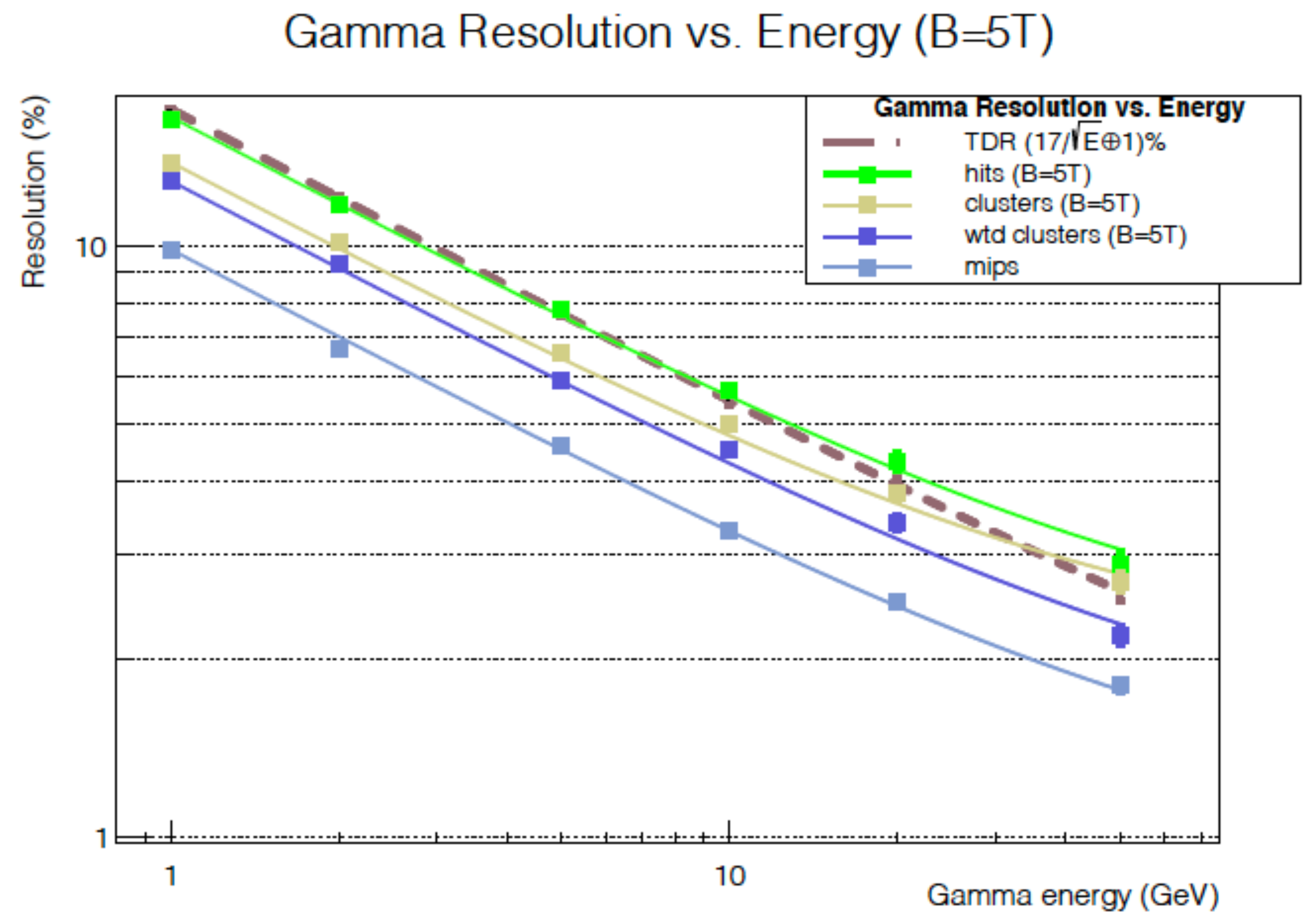
The goal in the search for an improved experimental resolution is to find an algorithm of the Hits which reaches as closely as possible to the MIPs performance, the assumed ideal performance. An initial improvement is achieved by combining Hits into clusters and counting clusters. A cluster is constructed by combining all Hits that touch each other on any of the eight connections, boundaries or corners. Figure 7 shows the distribution of cluster counts for 20 GeV gamma showers, and the number of MIPs contained within specific cluster counts. An additional improvement comes from noting the probability that multiple MIPs appear in clusters as a function of the cluster size and the cluster position in the shower, longitudinally and transversely. By applying both of these corrections, the 20 GeV gamma resolution is brought to 3.3%. The resulting energy-dependent resolution between 1 and 50 GeV is well characterized by 12.2%/ ⊕ 1.4%, compared to the MIP resolution of 9.8%/ ⊕ 1.1%.
Figure 8 shows the gamma energy resolution performance for the range of measurements from the basic MIP counting (light blue, an idealized, best possible resolution) to that achieved by analyzing Hits in clusters (dark blue). These simulations are now mature and are well positioned to guide the design and production of the sensors. Future planned simulation studies include optimized reconstruction of showers and s within jets, separation of electromagnetic showers and other depositions in the ECal, and the impact of these on jet energy resolution, particularly in the measurements of the Higgs branching ratios.
More generally, future work will include:
- Potential of multi-bit digital operation;
- Jet reconstruction;
- Optimization of the overall ECal design, including consideration of manufacturability, possible with robots.
The large volume of data provided by a MAPS-based ECal reveals details of particle showers. The extraction of the most pertinent information, e.g., particle energy, particle type, and the separation of nearby and overlapping showers, provides an opportunity to apply Machine Learning techniques. We plan to apply such deep learning methods to particle and jet reconstruction in the SiD collider detector ECal based on MAPS technology.
5. MAPS Performance for Tracker Detectors
A MAPS-based tracker for SiD would feature a sensor similar in size to that described in the ILC TDR, 10 × 10 cm2 devices. It would be constructed by stitching 2 cm × 2 cm reticles. However, such a device would provide exceptional granularity of 25 m by 100 m pixels, with the alignment placing the 25 m pixel dimension in the bend direction, providing a resolution of 25 mm without charge sharing. The 25 m pixel size matches the KPiX-readout, silicon-strip width of the SiD TDR design which was recently assembled, tested, and shown to achieve 7 m resolution [27]. The depleted 10 m thick epi-layer charge collection of the MAPS allows a minimum threshold of 1/4 MIP, ensuring high efficiency. The pixel nature provides vastly improved pattern recognition for track finding over the strip devices. For the endcaps, such a sensor would eliminate the need for two sensors in a small-angle-stereo configuration, reducing both the material budget and cost.
6. Summary
The application of MAPS in SiD tracking and ECal systems offers the potential for significantly improved performance from that envisioned in the ILC TDR [1]. Motivated by this, the SiD MAPS development targets improvements to speed and resolution performance, and the system approaches needed for large-scale use of MAPS at a reasonable cost. Beyond the linear collider, future colliders in general will need large areas of silicon sensors, several hundred m2, for low-mass trackers and sampling calorimetry. These developments, therefore, would have impacts beyond SiD. The requirements for trackers and calorimeters, particularly very thin, large areas with micron-scale resolution, are driving this work. An on-going effort focuses on developing readout electronics compatible with a power pulsing scheme: the analog front-end circuitry will be powered off during the dead-time between bunch trains. With low duty cycle machines such as ILC and C3, this technique reduces power by more than two orders of magnitude. The pixel front-end circuitry, as well, will be based on a synchronous readout architecture, where operation of the circuitry is timed with the accelerator bunch train. In this way, the noise and timing performance of the circuitry can be optimized while maintaining low-power consumption. The development of wafer-scale MAPS will allow designers to investigate the power pulsing, power distribution, yield, stitching techniques, assembly and power delivery.
Author Contributions
Conceptualization, M.B.; Investigation, A.H. and L.R.; Methodology, L.R.; Project administration, C.V.; Software, J.E.B.; Writing—original draft, J.E.B.; Writing—review & editing, J.E.B., M.B., C.V. and L.R. All authors have read and agree to the published version of the manuscript.
Funding
The authors were supported by the U.S. Department of Energy contract DE-AC02-76SF00515 and grant DE-SC0017996 for this research.
Data Availability Statement
The simulated data presented in the figures of this study are available on request from the corresponding author.
Conflicts of Interest
The authors declare no conflict of interest.
References
- Behnke, T.; Brau, J.E.; Philip N. Burrows, P.N.; Fuster, J.; Peskin, M.; Stanitzki, M.; Sugimoto, Y.; Yamada, S.; Yamamoto, H. The International Linear Collider Technical Design Report—Volume 4: Detectors. arXiv 2013, arXiv:1306.6329. [Google Scholar]
- Turchetta, R.; Berst, J.D.; Casadei, B.; Claus, G.; Colledani, C.; Dulinski, W.; Hu, Y.; Husson, D.; Le Normand, J.P.; Riester, J.L.; et al. A monolithic active pixel sensor for charged particle tracking and imaging using standard VLSI CMOS technology. Nucl. Instrum. Methods Phys. Res. Sect. A Accel. Spectrom. Detect. Assoc. Equip. 2001, 458, 677–689. [Google Scholar] [CrossRef]
- Deptuch, G.; Berst, J.D.; Claus, G.; Colledani, C.; Dulinski, W.; Gornoushkin, Y.; Husson, D.; Riester, J.-L.; Winter, M. Design and Testing of Monolithic Active Pixel Sensors for Charged Particle Tracking. IEEE Trans. Nucl. Sci. 2002, 49, 601–610. [Google Scholar] [CrossRef]
- Perić, I. A novel monolithic pixel detector implemented in high-voltage CMOS technology. In Proceedings of the 2007 IEEE Nuclear Science Symposium and Medical Imaging Conference, Honolulu, HI, USA, 26 October–3 November 2007; Volume 2, pp. 1033–1039. [Google Scholar] [CrossRef]
- Turchetta, R. Design and Process Development of CMOS Image Sensors with TowerJazz, Workshop on CMOS Active Pixel Sensors for Particle Tracking. 2014. Available online: https://indico.cern.ch/event/309449/contributions/1680002/attachments/591507/814229/cpix2014Turchetta.pdf (accessed on 7 September 2022).
- Deptuch, G.W.; Carini, G.; Enquist, P.; Grybos, P.; Holm, S.; Lipton, R.; Maj, P.; Patti, R.; Siddons, D.P.; Szczygiel, R.; et al. Fully 3D-integrated Pixel Detectors for X-Rays. IEEE Trans. Electron Devices 2016, 63, 205–214. [Google Scholar] [CrossRef]
- Greiner, L.; Anderssen, E.; Matis, H.S.; Ritter, H.G.; Schambach, J.; Silber, J.; Stezelberger, T.; Sun, X.; Szelezniak, M.; Thomas, J.; et al. A MAPS based vertex detector for the STAR experiment at RHIC. Nucl. Instrum. Methods Phys. Res. Sect. A Accel. Spectrom. Detect. Assoc. Equip. 2011, 650, 68–72. [Google Scholar] [CrossRef]
- Deptuch, G.; Winter, M.; Dulinski, W.; Husson, D.; Turchetta, R.; Riester, J.L. Simulation and Measurements of Charge Collection in Monolithic Active Pixel Sensors. Nucl. Instrum. Methods Phys. Res. Sect. A Accel. Spectrom. Detect. Assoc. Equip. 2001, 465, 92–100. [Google Scholar] [CrossRef]
- Deveaux, M.; Amar, S.; Besson, A.; Baudot, J.; Claus, G.; Colledani, C.; Deptuch, G.; Dorokhov, A.; Dulinski, W.; Goffe, M.; et al. Charge Collection Properties of Monolithic Active Pixel Sensors (MAPS) Irradiated with Non-Ionising Radiations. Nucl. Instrum. Methods Phys. Res. Sect. A Accel. Spectrom. Detect. Assoc. Equip. 2007, 583, 134–138. [Google Scholar] [CrossRef]
- Snoeys, W.; Rinella, G.A.; Hillemanns, H.; Kugathasan, T.; Mager, M.; Musa, L.; Riedler, P.; Reidt, F.; Van Hoorne, J.; Fenigstein, A.; et al. A process modification for CMOS monolithic active pixel sensors for enhanced depletion, timing performance and radiation tolerance. Nucl. Instrum. Methods Phys. Res. Sect. A Accel. Spectrom. Detect. Assoc. Equip. 2017, 871, 90–96. [Google Scholar] [CrossRef]
- Schioppa, E.J.; Tortajada, I.A.; Berdalovic, I.; Bortoletto, D.; Cardella, R.; Dachs, F.; Dao, V.; De Acedo, L.F.S.; Freeman, P.M.; Hemperek, T.; et al. Measurement results of the MALTA monolithic pixel detector. Nucl. Instrum. Methods Phys. Res. Sect. A Accel. Spectrom. Detect. Assoc. Equip. 2020, 958, 162404. [Google Scholar] [CrossRef]
- Contin, G. The MAPS-based ITS Upgrade for ALICE. arXiv 2020, arXiv:2001.03042. [Google Scholar]
- Mager, M. The LS3 upgrade of the ALICE Inner Tracking System based on ultra-thin, wafer-scale, bent Monolithic Active Pixel Sensors. In Proceedings of the 15th Trento Workshop on Advanced Silicon Radiation Detectors, Vienna, Austria, 17–19 February 2020. [Google Scholar]
- Prabket, J.; Poonsawat, W.; Kobdaj, C.; Naeosuphap, S.; Yan, Y.; Jeamsaksiri, W.; Yamwong, W.; Chaowicharat, E.; Hruanun, C.; Poyai, A. Resistivity profile of epitaxial layer for the new ALICE ITS sensor. J. Instrum. 2019, 14, T05006. [Google Scholar] [CrossRef]
- Theuvissen, A. BUTTING versus STITCHING (1). Available online: https://harvestimaging.com/blog/?p=1568 (accessed on 7 September 2022).
- Theuvissen, A. BUTTING versus STITCHING (2). Available online: https://harvestimaging.com/blog/?p=1599 (accessed on 7 September 2022).
- Wunderer, C.B.; Marras, A.; Bayer, M.; Glaser, L.; Gottlicher, P.; Lange, S.; Pithan, F.; Scholz, F.; Seltmann, J.; Shevyakov, I.; et al. The PERCIVAL soft X-ray imager. J. Instrum. 2014, 9, C03056. [Google Scholar] [CrossRef]
- Contin, G. The MAPS-based vertex detector for the STAR experiment: Lessons learned and performance. Nucl. Instrum. Methods Phys. Res. Sect. A Accel. Spectrom. Detect. Assoc. Equip. 2016, 831, 7–11. [Google Scholar] [CrossRef]
- Bai, M.; Barklow, T.; Bartoldus, R.; Breidenbach, M.; Grenier, P.; Huang, Z.; Kagan, M.; Lewellen, J.; Li, Z.; Markiewicz, T.W.; et al. C3: A “Cool” Route to the Higgs Boson and Beyond. arXiv 2021, arXiv:2110.15800. [Google Scholar]
- Brau, J.; Breidenbach, M.; Dragone, A.; Fields, G.; Frey, R.; Freytag, D.; Freytag, M.; Gallagher, C.; Haller, G.; Herbst, R.; et al. KPiX—A 1024 channel readout ASIC for the ILC. In Proceedings of the 2012 IEEE Nuclear Science Symposium and Medical Imaging Conference Record (2012 NSS/MIC), Anaheim, CA, USA, 29 October–3 November 2012; pp. 1857–1860. [Google Scholar]
- Dragone, A.; Caragiulo, P.; Markovic, B.; Herbst, R.; Nishimura, K.; Reese, B.; Herrmann, S.; Hart, P.; Blaj, G.; Segal, J.; et al. ePix: A class of front-end ASICs for second generation LCLS integrating hybrid pixel detectors. In Proceedings of the 2013 IEEE Nuclear Science Symposium and Medical Imaging Conference (2013 NSS/MIC), Seoul, Korea, 27 October–2 November 2013; pp. 1–5. [Google Scholar]
- Linssen, L.; Miyamoto, A.; Stanitzki, M.; Weerts, H. Physics and Detectors at CLIC: CLIC Conceptual Design Report. arXiv 2012, arXiv:1202.5940. [Google Scholar]
- Ballin, J.A.; Dauncey, P.D.; Magnan, A.M.; Noy, M.; Mikami, Y.; Miller, O.; Rajovic, V.; Watson, N.K.; Wilson, J.A.; Crooks, J.P.; et al. A Digital ECAL based on MAPS. arXiv 2009, arXiv:0901.4457. [Google Scholar]
- Stanitzki, M.; SPiDeR Collaboration. Advanced monolithic active pixel sensors for tracking, vertexing and calorimetry with full CMOS capability. Nucl. Instrum. Methods Phys. Res. Sect. A Accel. Spectrom. Detect. Assoc. Equip. 2011, 650, 178–183. [Google Scholar] [CrossRef]
- Dauncey, P.; SPiDeR Collaboration. Performance of CMOS sensors for a digital electromagnetic calorimeter. PoS 2010, 502, ICHEP2010. [Google Scholar]
- De Haas, A.P.; Nooren, G.; Peitzmann, T.; Reicher, M.; Rocco, E.; Rohrich, D.; Ullaland, K.; van den Brink, A.; van Leeuwen, M.; Wang, H.; et al. The FoCal prototype—An extremely fine-grained electromagnetic calorimeter using CMOS pixel sensors. J. Instrum. 2018, 13, P01014. [Google Scholar] [CrossRef]
- Brau, J.; Breidenbach, M.; Freytag, D.R.; Kleinwort, C.; Kraemer, U.; Reese, B.A.; Roelofs, S.; Stanitzki, M.; Steinhebel, A.; Tsionou, D.; et al. Lycoris—A large-area, high resolution beam telescope. J. Instrum. 2021, 16, P10023. [Google Scholar] [CrossRef]
Figure 1.
Cross-sections of MAPS structures and electric field lines in the improved process.

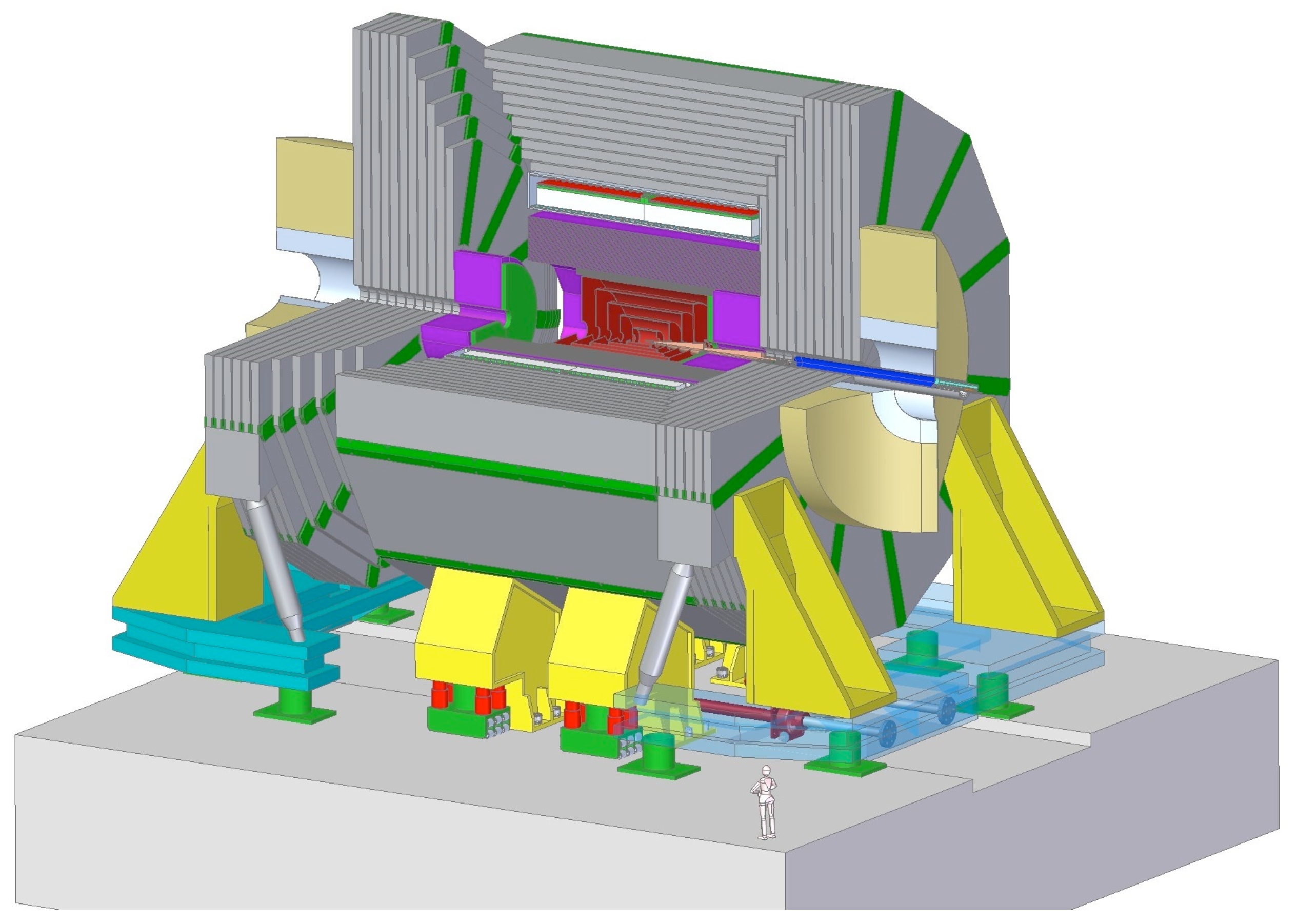
Figure 2.
SiD on its platform, showing tracking (red), ECAL (light green), HCAL (violet) and reconfigured dodecagonal iron yoke.
Figure 2.
SiD on its platform, showing tracking (red), ECAL (light green), HCAL (violet) and reconfigured dodecagonal iron yoke.

Figure 3.
The distribution of weighted (by longitudinal and transverse position in shower) cluster counts for a 10 GeV gamma shower in the new SiD digital MAPs design based on a Geant4 simulation.
Figure 3.
The distribution of weighted (by longitudinal and transverse position in shower) cluster counts for a 10 GeV gamma shower in the new SiD digital MAPs design based on a Geant4 simulation.

Figure 4.
Transverse distribution of two 10 GeV showers separated by one cm. LEFT: Pixel amplitudes in the ILC 13 mm TDR pixel design. RIGHT: Clusters in the first 5.4 radiation lengths in the new SiD digital MAPS design based on a Geant4 simulation.
Figure 4.
Transverse distribution of two 10 GeV showers separated by one cm. LEFT: Pixel amplitudes in the ILC 13 mm TDR pixel design. RIGHT: Clusters in the first 5.4 radiation lengths in the new SiD digital MAPS design based on a Geant4 simulation.

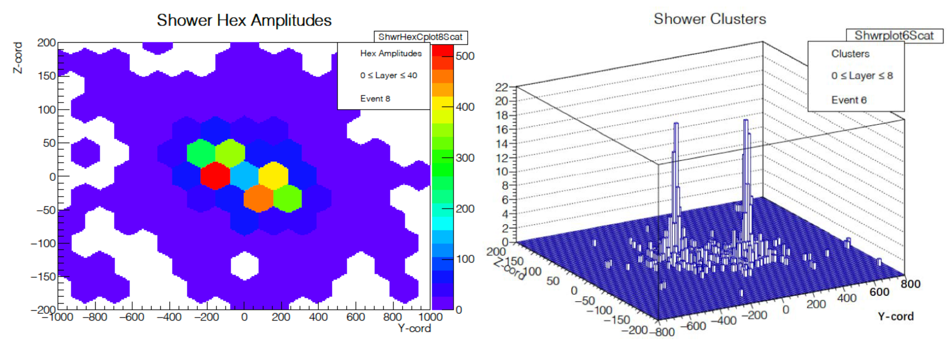
Figure 5.
Projection in z-layer plane of the pixel clusters in two 20 GeV gamma showers emerging from a 40 GeV decay. The z-direction is the 100-m pixel direction and the layers shown are 20 thin (0.64 X0) followed by 10 thick tungsten layers. Each vertical bin is 400 μm wide. The two showers are separated by less than one cm.

Figure 6.
Efficiency for distinguishing two 10 GeV electron showers as a function of shower separation (upper curve) and the degradation of energy resolution as a function of separation due to overlap of cluster hits (lower curve) in the new SiD digital MAPS design based on a Geant4 simulation.
Figure 6.
Efficiency for distinguishing two 10 GeV electron showers as a function of shower separation (upper curve) and the degradation of energy resolution as a function of separation due to overlap of cluster hits (lower curve) in the new SiD digital MAPS design based on a Geant4 simulation.

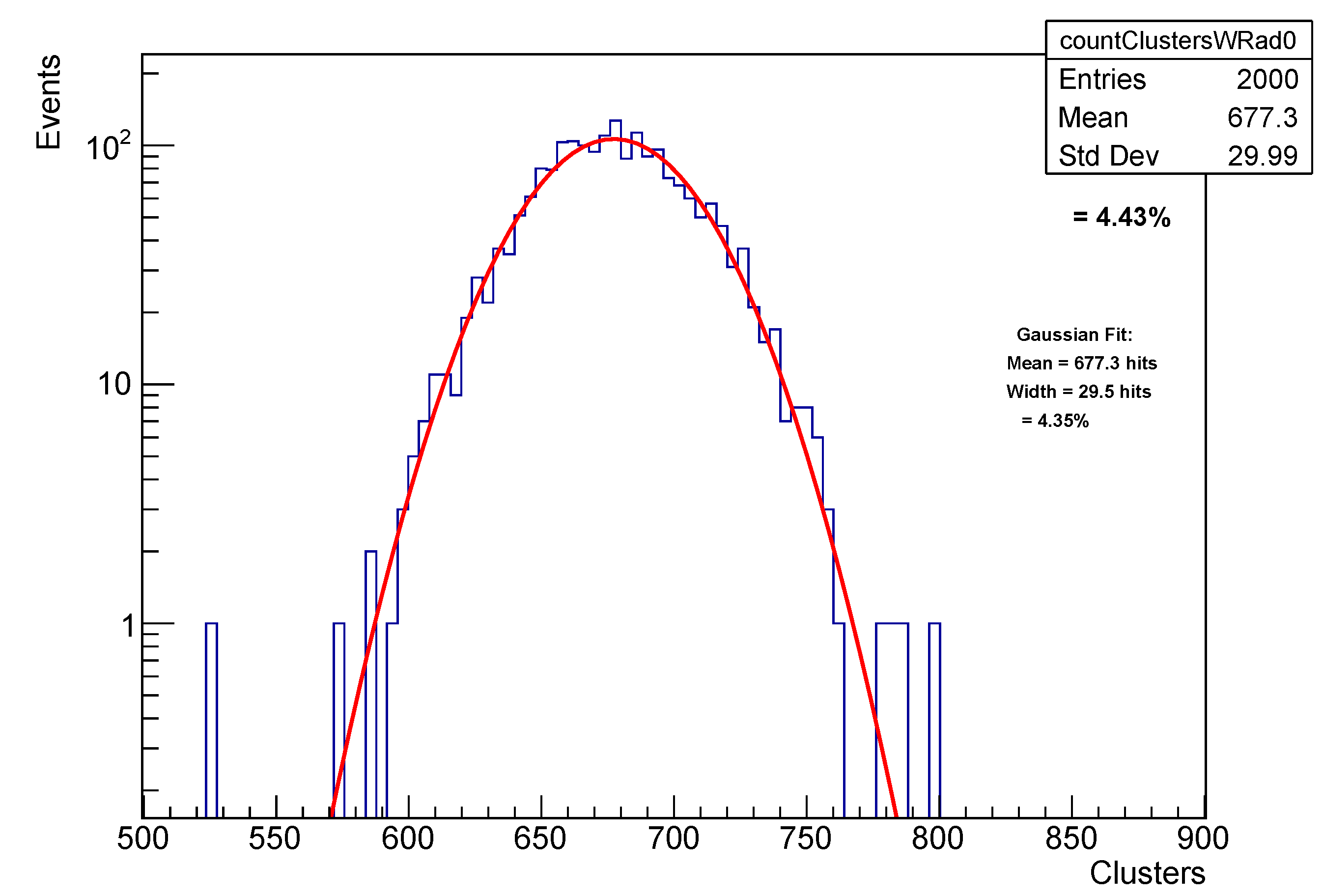
Figure 7.
Distribution of cluster counts for 2000 showers from 20 GeV gammas, and the number of MIPs contained within specific cluster counts.
Figure 7.
Distribution of cluster counts for 2000 showers from 20 GeV gammas, and the number of MIPs contained within specific cluster counts.

Figure 8.
Energy resolution for gamma showers as a function of energy. The curves show (from lower up) the resolution based on counting minimum ionizing particles (light blue, MIPs), modified cluster counting (dark blue), pure simple cluster counting (light brown), active pixels (green, Hits), and the required performance from the ILC TDR (brown dash–dot).


Table 1.
Target specifications for 65 nm prototype.
| Parameter | Value |
|---|---|
| Min. Threshold | 140 e− |
| Spatial resolution | 7 μm |
| Pixel size | 25 × 100 μm2 |
| Chip size | 10 × 10 cm2 |
| Chip thickness | 300 μm |
| Timing resolution (pixel) | ∼ns |
| Total Ionizing Dose | 100 kRads |
| Hit density/train | 1000 hits/cm2 |
| Hits spatial distribution | Clusters |
| Power density | 20 mW/cm2 |
Publisher’s Note: MDPI stays neutral with regard to jurisdictional claims in published maps and institutional affiliations. |
© 2022 by the authors. Licensee MDPI, Basel, Switzerland. This article is an open access article distributed under the terms and conditions of the Creative Commons Attribution (CC BY) license (https://creativecommons.org/licenses/by/4.0/).
Share and Cite
MDPI and ACS Style
Brau, J.E.; Breidenbach, M.; Habib, A.; Rota, L.; Vernieri, C. The SiD Digital ECal Based on Monolithic Active Pixel Sensors. Instruments 2022, 6, 51. https://doi.org/10.3390/instruments6040051
AMA Style
Brau JE, Breidenbach M, Habib A, Rota L, Vernieri C. The SiD Digital ECal Based on Monolithic Active Pixel Sensors. Instruments. 2022; 6(4):51. https://doi.org/10.3390/instruments6040051
Chicago/Turabian StyleBrau, James E., Martin Breidenbach, Alexandre Habib, Lorenzo Rota, and Caterina Vernieri. 2022. "The SiD Digital ECal Based on Monolithic Active Pixel Sensors" Instruments 6, no. 4: 51. https://doi.org/10.3390/instruments6040051