Magnetic Nanowires


Institute of Condensed Matter and Nanosciences, Université Catholique de Louvain, Place Croix du Sud 1, 1348 Louvain-la-Neuve, Belgium
Appl. Sci. 2020, 10(5), 1832; https://doi.org/10.3390/app10051832
Submission received: 19 December 2019
/
Revised: 16 January 2020
/
Accepted: 20 January 2020
/
Published: 6 March 2020
(This article belongs to the Special Issue State of the Art of Nanosciences in Belgium)
Abstract
:Magnetic nanowires are attractive materials because of their morphology-dependent remarkable properties suitable for various advanced technologies in sensing, data storage, spintronics, biomedicine and microwave devices, etc. The recent advances in synthetic strategies and approaches for the fabrication of complex structures, such as parallel arrays and 3D networks of one-dimensional nanostructures, including nanowires, nanotubes, and multilayers, are presented. The simple template-assisted electrodeposition method enables the fabrication of different nanowire-based architectures with excellent control over geometrical features, morphology and chemical composition, leading to tunable magnetic, magneto-transport and thermoelectric properties. This review article summarizing the work carried out at UCLouvain focuses on the magnetic and spin-dependent transport properties linked to the material and geometrical characteristics.
1. Introduction
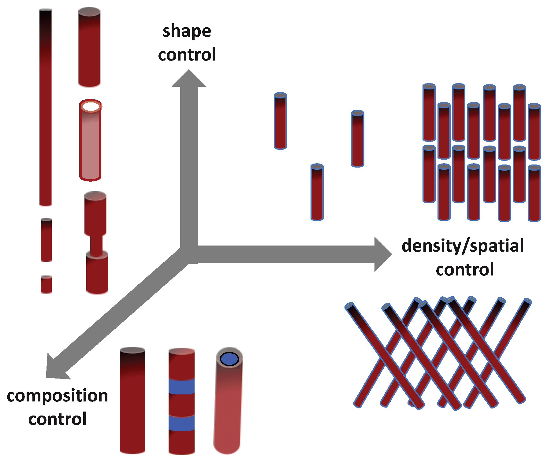
Over the last 25 years, the group at UCLouvain has developed a strong expertise in the template-assisted electrodeposition of elongated magnetic nanostructures such as homogeneous and multilayered nanowires (NWs) and nanotubes (NTs). Arrays of magnetic nanofibers with desired aspect ratio, composition, structure, morphologies and density were successfully synthesized by electrochemical deposition in nano-templates with well-defined pore architecture (see Figure 1). This template-assisted synthesis of nanowires has been demonstrated as a very powerful and versatile technique and has the merits of simplicity, high efficiency and low cost. These advantages are key elements compared to more complex and restrictive synthesis methods such as electron-beam lithography [1] and interference lithography [2,3]. Magnetic nanowires provide interesting physics and innovative ideas for fundamental studies in nanomagnetism and spintronics as well as for various device applications [4,5,6,7,8,9]. The group at UCLouvain has performed pioneering work on giant magnetoresistance (GMR) phenomena in magnetic multilayered NWs [5,10,11,12,13]. Extensive studies were realized on many ferromagnetic NW arrays using various experimental techniques for a deeper understanding of the magnetic properties and spin-dependent transport properties in relation with their nanoscopic dimensions [14,15,16,17,18,19,20,21,22,23,24,25,26,27,28,29,30,31,32,33,34,35,36,37,38,39,40,41,42,43,44,45]. The research activity at UCLouvain on magnetic NWs were also motivated by related applications in microwave devices [46,47,48,49,50,51,52,53,54] and multiferroic nanocomposites [55,56,57,58,59]. Recently, we demonstrated the suitability of three-dimensional (3D) nanoporous polymer templates to form dense interconnected magnetic NW networks with tunable geometrical parameters in terms of nanowire size, density, and orientation opens up the possibility for a controlled synthesis of a large variety of complex 3D networks of high aspect-ratio nanostructures with different geometries and materials [60,61,62,63,64,65,66,67]. Their unique architectures and high degree of nanowire interconnectivity facilitate the ability to perform magneto-transport measurements and to investigate the interplay between electronic and thermoelectric transport and magnetic properties.
The intent of this article is to provide a review of the most relevant results obtained by the group at UCLouvain on the fabrication, characterization and properties of ferromagnetic nanowires. The paper is organized as follows: first, the template-assisted electrodeposition methods which have successfully grown high quality parallel arrays and complex networks of nanowires, nanotubes and multilayers are briefly recalled in Section 2. The experimental investigations and analysis of the magnetic, magneto-transport and thermoelectric properties of single magnetic nanowires, nanowire arrays and nanowire networks are presented in Section 3. Finally, prospects of this field are outlined in Section 4.
2. Materials and Methods
Polymer membranes are made using the nuclear track-etch technology in which a film (typically 5–50 m thick) of polymer (polycarbonate, PET, polyimide, …) is bombarded by heavy ions of high energy [68]. The bombarded film is then irradiated with UV light to increase the track etching selectivity and finally etched in an adequate solution where tracks are revealed, leading to the formation of pores with a diameter defined by the etching time. Pore size and pore density can be controlled over wide ranges, between 15 nm and a few microns and in the range 10–10 cm, respectively. For such randomly distributed pores array, this implies that the mean separation distance between nanomaterials can be tuned between ∼100 nm up to several tens of microns, with a maximum porosity close to 30%. Porous alumina films formed by anodic oxidation of aluminum in an acidic solution have also been intensively used to fabricate nanostructured materials [69]. These templates contain cylindrical pores of uniform diameter oriented perpendicular to the surface and approximately arranged in a hexagonal array. The interpore distance and pore length increase in proportion to the applied anodization voltage and time, respectively. The pore diameter can be controllably increased by a pore widening treatment. Porous alumina with pore density as large as 10 and pore diameters ranging from approximately 5 nm up to >300 nm can be produced. Typical porosities are in the range 10–65%. It has also been shown that a two-step anodization process can lead to highly ordered two-dimensional pores arrays with a hexagonal pattern over large areas [70]. Figure 2a,b show the Scanning Electron Microscopy (SEM) images of the surface of the two types of porous templates. Electrochemical deposition of a material within the pores of polymer and alumina membranes is done by coating one face of the membrane with a sufficiently thick metal film to cover the pores and serve as a cathode for electrodeposition [5,10]. The nanoporous membrane is then placed in a home-made Teflon-cell and exposed to the electrolyte (see Figure 2c,d). A standard three-electrode setup is employed to reduce ions in solution at the cathode and make the nanowires. When necessary, the pH values of the as-prepared electrolytes were adjusted to the desired pH by addition of a diluted HCl solution or by addition of NaOH. Different types of parallel NW arrays made from pure metals, alloys of controlled composition and multilayered nanowires were successfully grown by electrodeposition at room temperature (RT) [5,10,23].
Typical SEM images of metal nanowires obtained via the simple potentiostatic mode after dissolution of the host nanoporous media are shown in Figure 3a,b. Note that, after the template is filled with magnetic wires, the term packing factor is used instead of the membrane porosity, since interest is focused on the properties of nanowire networks.
The technique mostly used for the fabrication of multilayered nanowires (see Figure 3c) consists in a pulse-plating method in which two metals are deposited from a single solution (in which the nobler element is kept in dilute concentration) by switching between the deposition potentials of the two constituents. Following a procedure described elsewhere [5,10], the deposition rates of each metals were determined from the pore filling time. This single-bath method was successfully used to prepare various multilayered nanowires including Co/Cu, NiFe/Cu, CoNi/Cu and Ni/Cu. Transmission Electron Microscopy (TEM) images of permalloy (Py = NiFe)/Cu and Co/Cu multilayered nanowires are shown in Figure 3d,e. Over the last decade, several groups also reported on the electrochemical synthesis of parallel arrays of Ni nanotubes within nanopores of anodic alumina oxide and polymer templates [42,44,71,72]. In this method, core-shell Cu/Ni nanocables are first grown in porous templates at a constant deposition potential, followed by the selective electrochemical etching of the Cu-rich core at an oxidation potential (see Figure 3f).
Most of the magneto-transport measurements were performed by simply contacting a small number of nanowires parallel to each other embedded in the porous matrix. However, measurements on single nanowires were also realized in previous studies [17,21,30,41,73]. Various experimental approaches have been developed for this purpose. For polymer templates with low pore density, a self-contacting technique [17,72] has been used successfully for contacting a single wire. For anodic porous alumina supported on Si substrate, nanolithography-based contacting techniques have been developed to allow the electrical connection of one single nanowire in a large assembly of wires [30,41]. Another approach is based on the use of electron beam lithography to connect a single nanowire after dissolution of the matrix that contains the nanowires [21].
Recently, 3D nanoporous templates were obtained by performing a sequential multi-step exposure of energetic heavy ions, at various angles with respect to the normal of polycarbonate film surface [60,74]. Then, the latent tracks within the polymer film were chemically etched following the previously reported protocol to obtain membranes with distinct porosities and pores sizes [68]. Hereafter, the as-prepared polymer membranes containing networks of interconnected cylindrical nanopores were designed with pores of well-defined diameters between 40 and 230 nm and with different porosity characteristics ( 3% and 20%, with P the void volume fraction of the membrane). Next, the template-assisted electrodeposition method was used for the synthesis of well-defined 3D architecture consisting of crossed nanowire (CNW) and nanotube (CNT) networks [60,61,62,63,66]. In addition, magnetic and non-magnetic layers were electrochemically stacked to make interconnected multilayered nanowires [64,65,67]. Figure 4 illustrates the various 3D nanofiber architectures which have so far been investigated. After electrodeposition, the complete dissolution of the PC template leads to an interconnected metallic self-standing structure, as the one observed for the 40 nm and 230 nm diameter Ni CNW network shown in Figure 4e–g. The CNW network exhibits the replicated complex nanowires branching morphology of the porous template.
The feasibility of using the same electrochemical method to fabricate large-scale 3D Ni CNT networks from Cu/Ni-core/shell nanocables was recently demonstrated [63]. This process results in Ni CNT networks as the one shown by the SEM micrograph reported in Figure 4h after dissolution of the host PC membrane. In addition, since the geometrical features of the crossed core(Cu)/shell(Ni) nanocables can be carefully modified via the control over the reduction or deposition potential, Ni CNT networks with different wall thickness in the range 10–50 nm were obtained after carrying out the dealloying step of the Cu core [63]. In addition, CNWs with multilayer structure of FM/Cu, with FM = Co, CoNi and NiFe alloys were fabricated in the host 3D porous templates [64,65,67]. Interestingly, this fabrication method appears as a very convenient approach for large scale production of current-perpendicular to-plane (CPP) giant magnetoresistance (GMR) films based on CNW networks, as shown in Section 3.3 and Section 3.5.
3. Results
3.1. Magnetization Reversal Processes in Magnetic Nanowires
Anisotropic magnetoresistance (AMR) arising from the relativistic spin-orbit coupling is a powerful tool for studying the magnetization reversal in magnetic nanowires. AMR is related to the dependence of the resistance on the angle between the magnetization of the ferromagnet and the electrical current direction. The change in resistance between current parallel and perpendicular to magnetization is often less than a few percent. However, as a high accuracy in the electrical resistance measurement can be obtained, AMR was used to investigate the reversal of magnetization of magnetic nanowires at different temperatures [17,73] and quantitative analysis of the results was conducted using classical models describing magnetization reversal. The magnetoresistive curve is related to the magnetization by
where is uniform and measured along the wire axis, is the saturation magnetization and is the angle between the applied field and the current (which is along the wire axis). In Equation (1), the quantity defines the AMR ratio. Figure 5a shows the magnetoresistive hysteresis loops obtained at room temperature on a single 75 nm Ni nanowire for the angles 10¼ and 75¼. Low density Ni nanowire arrays constitute an attractive model system in which the magnetization easy axis is simply determined by shape anisotropy.
As shown in Figure 5a, the AMR curves are composed of continuous variations of the resistance corresponding to a reversible rotation of the magnetization and of discontinuous jumps of resistivity at fields corresponding to magnetization reversal. It involves processes such as nucleation of small reversed domains at the end of the wire, before their possible expansion through domain-wall motion [14]. The jumps in AMR curves refer to successive pinning and depinning of the domain wall. The inset of Figure 5a shows a zoom in the region where the discontinuity occurs. Two resistance jumps appear for two field values that are close to each other. The first one refers to the nucleation of the magnetization reversal and propagation of a domain wall until it is trapped at a pinning center due to the presence of structural defects. The domain wall is evacuated when the external magnetic field reaches a higher field (giving rise to a second jump) where the magnetization of the wire is completely reversed. The nucleation field was measured on individual nanowires as a function of the angle between the applied field and the wire axis. The results were then compared with predictions of the micromagnetic theories. Figure 5b shows the dependence of the nucleation field Hn with the angle for the 75 nm-Ni nanowire. The angular dependence of the nucleation field is consistent with a process controlled by a curling rotational mode [14]. The results show that the magnetization switching is initiated by reversal inside some nucleation volume much smaller than the total volume of the nanowire [17,73]. For Ni nanowires, the measurements of the nucleation field as a function of temperature evidence an extra uniaxial anisotropy adding to shape anisotropy at low temperatures. By combining X-ray diffractometry, magnetization and ferromagnetic resonance measurements at different temperatures, this additional contribution was demonstrated to find its origin in magnetoelastic effects conjointly induced by the Ni and polycarbonate thermal-expansion coefficients mismatch and by the low volume fraction of Ni in the nanocomposite samples [16,31,40]. This additional magnetic anisotropy, whose magnitude is comparable to that of shape anisotropy, reinforces the wire axis as an easy axis for magnetization.
3.2. Tunable Magnetic Anisotropy of Magnetic Nanowire Arrays
The effective magnetic anisotropy in ensembles of parallel nanowires is determined by different contributions, namely shape anisotropy, dipolar interwire coupling, magnetocrystalline (MC) anisotropy and magnetoelastic terms. Magnetoelastic effects were found to be important only at low temperature in low porosity polymer membranes filled with Ni [16,40] and will be neglected hereafter. Consequently, the effective anisotropy field () with a uniaxial symmetry parallel to the wire axis is given by:
which includes the shape anisotropy for an infinite long cylinder, the dipolar coupling between the wires which lowers the magnetostatic energy and, in a mean field approximation, can be written as [19] (with P the packing factor of the nanowire array), as well as the possible contribution of a magneto-crystalline anisotropy that adds or competes with the shape anisotropy. Among the different approaches that have been used to investigate the static and dynamic properties of arrays of magnetic nanowires, ferromagnetic resonance (FMR) has proved to be a very powerful technique [19,23,24,29,32,34,35]. Indeed, at a given constant frequency f, the ferromagnetic resonance condition when the magnetic field is applied parallel to the wires is [19]:
where is the resonance field and the gyromagnetic ratio provides a direct and precise quantification of the effective field . Figure 6a shows typical microwave absorption curves measured on an array of 100 nm Ni nanowires ( 27%) as a function of the intensity of the static field applied parallel to the wires [19]. From these results, it can be seen that the absorption curves present an intense absorption peak which varies in position and intensity as the amplitude of the magnetic field is varied. Using porous membranes, the inter-wire spacing can be controlled over a wide range. This allows to explore the properties and dipolar interactions between the wires from the limit of isolated towards the limit of almost touching wires [19]. In Figure 6b–d, we present the dispersion relation and the corresponding hysteresis loops, measured with the magnetic field applied parallel (closed symbols) and perpendicular to the wires (open symbols) for three different Ni samples having a diameter and packing density of (b) 180 nm and 4%, (c) 100 nm and 27% and (d) 115 nm and >35%. The data were compared to the calculated ones for isolated wires, shown as solid lines. For low packing densities, the measured resonance frequencies in the saturated states agree well with the values expected for an array of isolated wires, see Figure 6b. At higher wire density for both field directions, the measured frequencies are almost identical, as shown in Figure 6c. In addition, above a critical value of the packing (estimated around 33% for an ordered nanowire array), there is a tilt of the easy axis of magnetization between directions parallel to perpendicular to the wire axis, as shown in Figure 6d. Therefore, by increasing the density of the NW array, it is possible to modulate the effective magnetic anisotropy, from the case of isolated wires with the easy axis parallel to the wires to dense NW arrays in which the easy axis is perpendicular to the wires, passing through the particular case of quasi-isotropic magnetic systems. The observed deviations from the frequency-field dispersion curves calculated in weak field conditions are due to the fact that the system is no longer single-domain.
A control of the effective magnetic anisotropy can be achieved not only by changing the packing factor nanowire arrays but also by tailoring the magnetocrystalline anisotropy, as demonstrated for Co [24,29] and CoPt [28] nanowire systems. From our previous studies, the electrolytic bath acidity, or pH, was demonstrated to be a key parameter in determining the structure of electrodeposited cobalt nanowires. Indeed, it was found that face-centered cubic (fcc) Co is favored at low pH (typically less than 2.5) while hexagonal close-packed (hcp) Co is formed at pH larger than ∼3.5 [24,29]. Moreover, it was shown that an abrupt transition in crystallographic orientation takes place for pH in the range 4.0–6.5, with a preferred in plane orientation at low pH and a reorientation of the c-axis normal to the film at large pH. These structural changes have been attributed to the influence of evolution of hydrogen at the cathode, which are known to depend on the pH [75,76]. Another relevant parameter of the operative conditions in cobalt electrocrystallization is the current density.
Figure 7a shows the variation of the effective field for a 30 nm Co nanowires array as a function of the pH in the range 2.0–6.6 for two different plating current densities, around 50 mA·cm and 5 mA·cm, respectively. These data were extracted from FMR experiments [24,29]. Let’s first consider the results obtained at 50 mA·cm. For reference, the effective field 8 kOe expected when there is no contribution from the MC anisotropy is indicated by the dotted line in Figure 7a ( 3% is for the array samples in this study). This value agrees with that of the low-pH samples, for which only the shape anisotropy and dipolar coupling should be considered due to the lack of texture in the electrodeposited Co microstructure and possible presence of fcc phase. In contrast, for pH values of 3.8–4.0, it was found that the microstructure of the deposited Co nanowires contains a dominant fraction of large hcp grains with the c-axis oriented perpendicular to the wire. A similar result was observed for all the diameters considered in the range 30–120 nm [24,29]. For such samples, the effective anisotropy field is weaker than for the low-pH samples due to the competition between shape anisotropy and MC anisotropy (which has an upper bound of 6.4 kOe for bulk hcp Co). Moreover, a re-orientation of the hcp c-axis along the wire axis is also observed for pH values ≥ 6.0 [24], resulting in an additive MC contribution to the total anisotropy field.
For both low and high plating currents, the overall variation of the effective field with bath acidity is similar, see Figure 7a. However, the transition between the low and high effective fields takes place around different pH values depending on the plating current density. Therefore, for a limited pH range, it is possible to selectively obtain both structural phases (c-axis parallel and perpendicular to the wires) from the same electrolyte simply by changing the plating current (or deposition rate). These results are corroborated by TEM investigations as shown in Figure 7b,c [29]. In the case of low current density, the TEM bright field images and corresponding diffraction patterns clearly show an orientation of the c-axis parallel to the wire axis, while, in the case of high current density, the images clearly show a perpendicular orientation of the c-axis.
CoPt alloy nanowires constitute another system whose magnetic anisotropy can be changed drastically by appropriate annealing treatment after electrodeposition. These interesting properties of CoPt alloys are related to its ordered face centered tetragonal (fct) phase (L1) which exhibits very large magnetocrystalline anisotropy energy (up to 5 × 10 erg·cm around the equiatomic region). For this purpose, we used a thin anodized aluminum oxide film template (1.5 μm thick) on a doped silicon wafer, which affords the thermal durability of the nanoholes for high temperature process after electrodeposition. The as-made electrodeposited 80 nm CoPt nanowires were magnetically soft as shown by the hysteresis loops in Figure 8a. The large packing in the array (close to 50%) induces a strong interwire dipolar coupling that overcomes the shape anisotropy, thus resulting in an easy axis perpendicular to the wire axis. Appropriate thermal treatment at 700 ¼C has contributed to ordering the alloy nanowires. X-ray diffraction patterns have confirmed that the L1 ordered phase was successfully obtained in such CoPt nanowires [28]. Hysteresis loops of the annealed sample measured parallel and perpendicular to the wires are displayed in Figure 8b. Magnetic hardening is developed after annealing at 700 ¼C with coercive fields as large as 11 kOe at room temperature. No anisotropy exists between the two directions, although the length/diameter ratio of the wires is larger than 10. This is because the L1 CoPt has a strong MC anisotropy, much higher than the shape anisotropy. In addition, the nanowires are textured along the <111> direction which makes an angle of 55¼ with the (001) easy axis, resulting in an absence of anisotropy.
3.3. Spin Transport in Multilayered Nanowires
Multilayered nanowires are ideal structures to investigate the giant magnetoresistance (GMR) and its temperature dependence in the Current Perpendicular to the layer Plane (CPP) geometry. The first measurements were performed in 1994 on Co/Cu nanowires by Piraux et al. [10], Blondel et al. [77] and Liu et al. [78]. Nanowire systems have key advantages over conventional magnetic multilayers made by vacuum deposition. Firstly, the electrodeposition method into porous templates is much more convenient than vacuum deposition techniques for making multilayers with layer thicknesses close to the micron without degrading the quality of the interfaces. As a result, measurements on nanowires have been very useful to study the regime with layer thicknesses above the spin diffusion length (SDL), to test the theoretical predictions in this regime and to determine the SDL of various materials. Secondly, most of the measurements in CPP geometry on planar multilayers were performed with superconducting niobium contacts. Such measurements are therefore limited to the helium temperature range. On the other hand, measurements on nanowire systems can be carried out up to the ambient temperature, which has made it possible to study the temperature dependence of CPP-GMR [79]. Third, a high aspect ratio of the multilayered nanowires leads to large signals and precise measurements. Up to now, most measurements have been performed on Co/Cu, CoNi/Cu, Py/Cu systems and FeCoNi/Cu [10,11,77,78,79,80,81,82,83]. In Figure 9a, we show an example of CPP-GMR curves obtained for a Py/Cu multilayered nanowires sample. The MR ratio reaches 67% at 77 K and 71% at 4.2 K. Another example of experimental results for Co/Cu nanowires is also shown in Figure 9a. In both cases, the thickness of each FM/Cu bilayers is about 15 nm.
Most measurements on multilayered nanowires have been analyzed using the Valet–Fert model [84,85]. This model takes into account the important effects due to the spin accumulation occurring at the interfaces when the conduction in the ferromagnetic layers is spin dependent. In addition to the usual relaxation term for the momentum, the Boltzmann equation of the Valet–Fert model also includes a spin-lattice relaxation term describing the relaxation of spin accumulation by spin-flip scattering. In the case of multilayers with thick ferromagnetic layers, the GMR contribution from bulk scattering dominates that from interface scattering. For FM/Cu multilayers, if FM layers are thicker than the spin diffusion length in FM, and Cu layer much thinner than the one in Cu, the CPP-GMR ratio can be expressed as [5]:
with ( and are the corresponding resistances for antiparallel and parallel arrangements, respectively), the bulk scattering spin asymmetry coefficient (), the spin diffusion length in the FM material, the thickness of the FM layers and p the proportion of antiparallel orientations of the magnetization in consecutive magnetic layers. The spin asymmetry coefficients are usually determined from analysis of the experimental results in the long SDL limit (, ). Typical values are 0.35–0.5 for Co and 0.7–0.8 for Py. Equation (4) expresses that only a depth on both sides of a magnetic layer is “active” in this limit. The variation as of Equation (4) is illustrated by the experimental results of Figure 9b for Co/Cu multilayers. Once p is determined by independent Magnetic Force Microscopy observations, the variation of Figure 9b can be used to derive the SDL length in Co, 59 nm at 77 K [5]. At room temperature, 40 nm. In Figure 9c, we show another example of variation of the GMR as for a collection of Py/Cu/Py trilayers [5]. The SDL in Py, 3.3 nm 5.3 nm, has been derived from an analysis of these data with an expression similar to Equation (4). This value is in approximate agreement with that found for planar multilayers [86], 5.5 nm.
Despite their complex nano-architecture, interconnected NW networks made of Co/Cu, CoNi/Cu and Py/Cu multilayers were found to exhibit very large CPP-GMR responses reaching values of 40% at RT and 86% at 15 K for CoNi/Cu [64]. The same features were observed on the Co/Cu and Py/Cu CNW samples [65,67], as shown in Figure 10a–c.
The effects related to spin-transfer torque from a spin-polarized current in a nanosized ferromagnet have been studied in specially designed nanowires containing Py/Cu/Py and Co/Cu/Co pseudo spin-valves electrodeposited in anodic porous alumina supported on Si substrate (see Figure 11a). Single nanowire electrical connection techniques were developed for this purpose [30,36,41]. Switching phenomena driven by a spin-polarized current were clearly demonstrated in Py/Cu/Py trilayer nanowires [30].
In Figure 11b, we show the variation of the differential resistance ddI versus injected direct current at small magnetic field. Starting from the P state at zero current, the injected current is first decreased toward negative values. We first observed a sharp increase of the resistance at −2.5 mA due to the magnetization switching of the thin Py layer. The curve is hysteretic because the system remains in this high resistance state until the current is swept to a positive value. At a critical positive current of about +0.4 mA, the resistance flips back to the P state level. The system remains in this low resistance state at higher positive current. In addition, under specific magnetic field and injected current conditions, emission of microwave current was detected in Co/Cu/Co pseudo spin-valves with frequency in the GHz range and linewidth as low as 1.8 MHz [37,41,45]. Microwave signals have been obtained even at zero magnetic field and high frequency versus magnetic field tunability was demonstrated. From micromagnetic simulations, it appeared that the microwave emission is generated by the vortex gyrotropic motion which occurs in, at least, one of the two magnetic layers of our spin-valve structures. To stabilize the magnetic vortex state, a saturating perpendicular magnetic field is first applied to the sample before a decreasing ramp of magnetic field. The results reported in Figure 11c for the measured spin-transfer nano-oscillator containing a single spin-valve are related to the two-vortex state with vortices of opposite polarity present in both the magnetic layers of the spin-valve. The magnetic states responsible for the microwave emission were found to be consistent with micromagnetic simulations [37,41,45]. This bottom-up approach is promising for microwave device applications since it allows connection of dense arrays of stacked metallic spin valves in series and/or parallel, which could lead to high-quality coherent emission by synchronization.
3.4. Interplay between the Magnetic and Magneto-Transport Properties in Interconnected Nanowire Networks
In this section, we report on magneto-transport measurements performed on homogeneous CNW networks (40 nm diameter) made from CoNi alloys, while sweeping the magnetic field in the out-of-plane (OOP) and in-plane (IP) directions. In this system, the magnetic anisotropy has been found to be dependent on the alloying composition. The experimental setup for magneto-transport shown in Figure 12a is based on a two-probe system created at the surface of the filled template by local removing of the cathode by plasma etching. In this configuration, the current is directly injected to the branched CNW structure from unetched sections of the metallic cathode and goes through the network thanks to the high degree of electrical connectivity of the CNWs. Figure 12b,c show resistance curves measured at 290 K with the external field applied in the OOP and IP directions for interconnected NiCo CNW networks. As observed in Figure 12b, the maximum resistance in the Ni-rich NiCo sample is reached near zero applied field for both directions, which is consistent with remanent magnetization states where the magnetization tends to be aligned along the nanowire axis, due to shape anisotropy. Conversely, the decrease of the resistance near zero field in the Co-rich NiCo sample (see Figure 12c) is consistent with the decrease of the remanent magnetization as a result of the misalignment of the magnetization with respect to the NWs axis. Indeed, decreasing the Ni content below 45% leads to the appearance of a transverse hcp magnetocrystalline anisotropy contribution, which competes with the magnetostatic anisotropy contribution, since the c-axis is perpendicular to the nanowires axis, as revealed by XRD analysis [61,62].
Therefore, the magnetic anisotropy in OOP of Ni-rich networks is higher than that of Co-rich ones, as expected. Figure 12d shows the MC field as a function of the Ni content (x), obtained by FMR measurements on several NiCo CNW networks. As expected, is negative and increases toward the observed limiting value for pure Co networks with perpendicular c-axis as the Ni content is reduced. It is worth mentioning that the small negative anisotropy contribution observed for the Ni sample could be originated by residual stresses due to the reduced diameter of the nanowires, as recently suggested [87]. Figure 12e shows the anisotropic magnetoresistance ratio (AMR) vs. Ni content (x) at 20, 150 and 290 K for the different NiCo CNW networks (See [61,62] for more details on the estimation of AMR ratio in such CNWs). The observed variation of the AMR ratio as a function of x is consistent with previous reports on electrodeposited films and metallurgically processed NiCo alloys [88,89,90], where the maximum at x ∼ 75% for both temperature values is attributed to a magnetostriction and MC constants close to zero and to a saturation magnetization of about one Bohr magneton per atom for that particular alloy composition [90].
It is interesting to note that a close relation between the CNWs magnetic and structural properties has also been found in Co CNWs networks (40 nm diameter) where the effective magnetic anisotropy can be strongly modified using well-known mechanisms to modify their microstructure, such as the electrolyte pH [61]. Overall, the results obtained in Co CNWs are in very good agreement with the previous results obtained in arrays of parallel Co NWs [24]—see Section 3.2.
3.5. Spin Caloritronics in Nanowire Networks
A current trend is pushing the development of the next generation of thermoelectric materials to exploit spin-based transport mechanisms [91]. In this context, the coupling of thermal transport with spintronics is at the heart of the emerging field of spin caloritronics [92,93]. Previous studies on metallic nanostructures, magnetic tunnel junctions and magnetic insulators have led to the observation of several novel physical phenomena that may differ strongly from conventional thermoelectric effects such as Seebeck spin effects [94,95], thermally controlled spin injection [96] and thermally assisted spin transfer torque [97,98]. However, the low conversion efficiency of the observed effects and the low power of spin caloritronic devices greatly limit the spectrum of applications. Another difficulty is the lack of experimental approaches for reliable measurements of spin caloritronic material parameters. It has recently been shown that arrays of interconnected nanowires embedded in porous polymer films provide a simple and cost-effective way to fabricate flexible spin caloritronic devices at the macroscopic scale [64,65].
The diffusion thermopower arises from a diffusion of charge carriers opposite to the temperature gradient. It is related to the energy dependent conductivity of the material by Mott’s formula:
with VK the Lorenz number and e the electron charge (positive). According to Einstein’s relation for a metal or alloy with isotropic properties, the conductivity is proportional to the density of states and to the scattering time , where both terms are to be evaluated at the Fermi level . Because of the pronounced structure of the d-band and the high energy derivative of the density of states at the Fermi level in 3d ferromagnetic metals, large diffusion thermopowers are obtained (e.g., −30 V/K in cobalt at RT). In addition, these magnetic metals exhibit significant magnon–drag contribution to the thermoelectric power within a wide temperature range [99,100]. Importantly, the largest RT thermoelectric power factor (PF , with the electrical conductivity), which is the physical parameter that relates to the output power density of a thermoelectric material, is achieved for Co (PF ≈ 15 mW/Km) [101].
In multilayer stacks made of ferromagnetic (FM) metals and Cu, the Seebeck coefficient in a direction perpendicular to the layers can be calculated from the corresponding transport properties using Kirchhoff’s rules [102],
where and represent the thermopower and the thermal conductivity of the ferromagnetic material and Cu and the thickness ratio of FM and Cu layers. In metals, heat conductivity is primarily due to free electrons. Therefore, considering FM/Cu multilayers and using Wiedemann–Franz law ( where L is the Lorenz ratio), Equation (6) simply reduces to
with and the corresponding electrical resistivities. According to Equation (7), is mainly determined by the large thermopower of the FM metal in case the thickness ratio is not too small since . The same conclusion is drawn when the FM layer is formed from alloys such as CoNi and NiFe because of highly contrasting thermal conductivity values between the alloy and Cu. In contrast, the Seebeck coefficient of a FM/Cu multilayer stack in the direction parallel to the layers is given by
showing that large thermopower can be obtained only in case the thickness ratio is very large. The contrasting behavior between layer parallel and perpendicular directions is illustrated in Figure 13a for Co/Cu multilayers using Equations (7) and (8) and the literature resistivity and thermopower values at RT. The device configuration to measure the Seebeck coefficient and the magnetothermoelectric effect is schematically represented in Figure 13b. In such centimeter-scale nanowire networks, electrical connectivity is essential to allow charge and heat transfer over the whole sample sizes. Heat flow is generated by a resistive element and a thermoelectric voltage is created by the temperature difference between the two metallic electrodes that is measured by a thermocouple (see [64] for details). For conducting thermoelectric and magnetoresistance measurements, the cathode was locally removed by plasma etching to create a two-probe design, with the flow of current restricted along the nanowire segments, thus perpendicularly to the plane of the layers in FM/Cu CNWs. As shown in Figure 13c,d, the resistance and thermopower of the low-packing density ( 3%) Co/Cu NW sample (80 nm in diameter) show the same magnetic field dependencies and similar relative changes of ∼25% at 8 kOe at RT. The samples are nearly magnetically isotropic, as observed from the magneto-transport curves obtained with the applied magnetic field along the OOP and IP directions of the NW network films (see Figure 13c,d). This behavior corresponds to the one expected considering the CNW architecture and magneto-static arguments when using similar magnetic and non-magnetic layer thicknesses [32]. In the following, only the measurements obtained in the plane of the CNW network films are reported. Recent estimations of the thermoelectric power factor at RT for both Co/Cu and CoNi/Cu CNW networks lead to values around 5 mW/Km in the saturated state [64,65], which are even larger than the PF of the widely used thermoelectric material, bismuth telluride (in the range 1–5 mW/Km) [103]. In addition, the PF values obtained for FM/Cu NW networks embedded in polymer membranes are at least one order of magnitude larger than those of flexible thermoelectric films based on optimized conducting polymers, namely PEDOT-Tos films [104]. Very large magneto-power factor, reaching 100% at RT, was obtained for the Co/Cu CNWs. On the other hand, the efficiency of a material’s thermoelectric energy conversion is determined by its figure of merit . Due to the very low thermal conductivity of polycarbonate ( 0.2 W/m·K at RT), the contribution of the polymer matrix to heat transport is much smaller than that of the metallic nanowire network. In this case, the figure of merit is reduced to , thus leading to 1.6 × 10 ( 1.9 × 10) for the Co/Cu (CoNi/Cu) NW network sample at RT [64,65]. Although the figure of merit is more than one order of magnitude smaller than those of state-of-the-art thermoelectric materials ( 1 in BiTe alloys), it is comparable to those of thermocouple alloys ( 6 × 10 and 1.4 × 10 in constantan and chromel, respectively) and can be used in applications for devices with low energy requirements when the supply of heat essentially is free as with waste heat.
In the limit of no-spin relaxation, most of the CPP-GMR data can be understood using a simple two-current series-resistor model, in which the resistance of layers and interfaces simply add and where ’up’ and ’down’ charge carriers are propagating independently in two spin channels with large spin asymmetries of the electron’s scattering [105,106]. Similarly, significantly different Seebeck coefficients for spin-up and spin-down electrons, and , are expected because the d-band is exchange-split in these ferromagnets, as suggested from previous works performed on dilute magnetic alloys [107,108]. Assuming that the layers of the magnetic multilayers are thin compared to the spin-diffusion lengths and according to the usual rule when the currents split to flow along two parallel paths (see Figure 14a), the corresponding thermopowers and in the high- and low-resistance states, respectively, are simply given by [109]:
and
where separate resistivities and and Seebeck coefficients and are defined for majority and minority spin channels. Therefore, the spin-dependent Seebeck coefficients can be expressed as follows:
where denotes the spin asymmetry coefficient for resistivity. From Equations (11) and (12), it can be easily deduced that and in the limit of an extremely large MR ratio ( 1). Figure 14b shows the temperature evolutions of , , and for CoNi/Cu CNWs using a rough estimate of . Below RT, the various Seebeck coefficients decrease almost linearly with decreasing temperature, which is indicative of the dominance of diffusion thermopower. Similar results were obtained on Co/Cu CNWs (not shown in Figure 14). From the analysis, the estimated values for of V/K and V/K for Co/Cu and CoNi/Cu CNWs, respectively, are much larger than the one of μV/K extracted from measurements performed on Co/Cu/Co nanopillar spin valve using a 3D finite-element model [96,110].
Recently, we have demonstrated the fabrication of nanowire arrays based on diluted NiCr and CoCr alloys by electrodeposition in 3D porous membranes [66]. Measurements of magnetoresistance and thermoelectric power were performed as a function of temperature and chromium content in these diluted alloys. The changes in sign observed in the Seebeck coefficient and in the anisotropic magnetoresistance were related to significant changes in the density of the for the majority spin electrons. The evolution of the MR ratio with respect to the Cr content for NiCr NW networks is shown in Figure 15a at RT and 100 K. For all samples, positive values are found at RT, showing a rapid decrease in MR with the increasing Cr concentration. In contrast, the negative MR ratio was measured at 100 K for the NiCr sample with 4 and 7 at.% of Cr. The inset in Figure 15a shows that the MR ratio of the NiCr NW sample gradually increases from its negative value at low temperature to positive values for 150 K. In contrast, CoCr alloy NWs display negative AMR at RT for a Cr concentration ≥ 3 at. %. Negative values are also obtained at 100 K for all CoCr NW samples, and the absolute values for MR at low temperatures are almost independent of the alloy content even for a Cr concentration as small as ∼ 1at.%. The inset of Figure 15b shows the gradual change in the sign of MR(T) for the sample with the lower Cr concentration (CoCr). Overall, our experiments performed on both NiCr and CoCr alloy NW networks are in qualitatively good agreement with the model predictions of Campbell, Fert, and Jaoul [111,112]. In this simplified model, the sign of the AMR ratio has been tentatively linked to the value of the spin asymmetry coefficient in the alloy through a model based on a spin–orbit mechanism. The model predicts that at low temperatures, the AMR is proportional to the quantity , and so a negative AMR ratio is expected when electronic conduction is dominated by minority spin electrons, as expected for dilute NiCr and CoCr alloys. Moreover, the experimental results obtained at low temperature on CoCr NWs follow the prediction of MR being independent of the impurity concentration, as shown in Figure 15b. The influence of the impurity concentration on the thermoelectric power has been also investigated. Figure 15c,d show the variation of the Seebeck coefficient with the Cr content at some selected temperatures in the absence of any external magnetic field. As shown in Figure 15c, the thermopower of NiCr suddenly changes sign from negative to relatively large positive values with the addition of Cr impurities in Ni. The RT Seebeck coefficient goes from −20 V/K to about +17.5 V/K for the NiCr alloys with 7 at.% of Cr. Similar changes in thermopower sign have been reported in bulk NiCr alloys where minority spin dominates the electrical conduction [107,108,113]. The sign inversion of the Seebeck coefficient from negative to positive in dilute NiCr alloys could also be explained on the basis of a virtual bound state passing through the Fermi level in the spin up band [107,108]. In contrast, the sign of the Seebeck coefficient does not change for any value of Cr concentration for CoCr NW networks (see Figure 15d). The RT thermopower drops rapidly from V/K for pure Co to much smaller negative values approaching V/K for CoCr NWs. The CoCr NW samples are found to exhibit the same features at lower temperatures, as also shown in Figure 15d. Finally, the high room-temperature power factors of these magnetic nanowire networks (estimated in the range of 1–10 mW/Km [66]) provide interesting perspectives for designing n- and p-type legs for flexible spin thermoelectric devices.
Current flow in high-packing density NW networks (P = 20%) results in Joule heating as well as a Peltier heat current at the junctions between the NW network and the gold electrode, as recently demonstrated [65]. These heat flows were evaluated from the temperature changes for different current intensities and polarities, as well as for various applied magnetic fields (see Figure 16a). In the case when the DC current flows from the NWs (with the higher Peltier coefficient) to the gold electrode (with the lower one), we found that the Peltier heat is released from the junction, i.e. net cooling happens. As expected, the situation is reversed when the current flows in the opposite direction. In our experiments [65], the Peltier cooling ability of Co/Cu CNW network was estimated to be around 8.5 K/A.
As shown in Figure 16b, the magneto-Peltier effect has been quantified by recording the temperature change during the magnetic field sweeps. The field dependence of resembles that of MR. Since currents up to few hundreds mA are able to pass through the densely packed NW films without damaging the network structure, we estimated that a magnetic field can switch a heat flow as large as 1 mW.
4. Discussion
The research activity developed at UCLouvain over the last 25 years on magnetic nanowires opens up the possibility for a controlled template-assisted synthesis of complex nanowire-based architectures with excellent control over geometrical features, morphology and chemical composition, leading to tunable magnetic, magneto-transport and thermoelectric properties. Due to their relative ease of fabrication, magnetic nanowires are promising materials for a variety of applications, ranging from magnetic, high frequency and electronic devices to sensing and bio-applications. On the road towards the size reduction of microwave devices, ferromagnetic nanowires embedded into porous templates have also proven to be an interesting alternative route to ferrite based materials. The main advantages of magnetic nanowired substrates compared to classical ferrites are a higher operation frequency and a microwave absorption without application of an external magnetic field as these NWs behave as strong uniaxial nanomagnets. In contrast, standard ferrite devices such as non-reciprocal devices need to be biased by a magnetic field provided by a permanent magnet to operate. In close collaboration with Prof. I. Huynen at UCLouvain, we have successfully prepared a variety of FM nanowire based substrates and demonstrated the ability to build planar reciprocal and non-reciprocal devices for very high frequencies, such as phase shifters, isolators or circulator [46,47,48,49,50,51,52,53,54] (see Figure 17). More recently, we also demonstrated the operation of fully integrated and miniaturized waveguides based on ferromagnetic nanowires used as microwave isolators. Nanowires of various heights were selectively grown at dedicated areas into nanoporous alumina template in order to create the shielding walls of a Substrate Integrated Waveguide (SIW) topology and the ferromagnetic slab supporting a circularly polarized nonreciprocal propagation [52]. Tremendous advantages can be expected in terms of ease of integration and power consumption.
Spin-valve nanopillars such as Co/Cu/Co and NiFe/Cu/NiFe are also ideal devices to achieve high injection current densities and are very promising for applications as spin transfer nano-oscillators (STNOs). The sustained gyrotropic mode of vortex magnetization in these segmented nanopillars provides improved spectral quality microwave signals without any static bias magnetic field. Lithography techniques allow you to connect a single or a desired number of spin-torque vortex oscillators from the dense forest-like structure of nanowires embedded in nanoporous alumina templates integrated onto Si wafers, with better compatibility to the standard CMOS processes. The prospect of obtaining the synchronization of a large number of STNOs, either along the same wire or in neighboring wires, is interesting in order to achieve the required power for applications. Magnetic nanowires embedded in a polymer membrane could also be used to develop various light weight and flexible magnetic sensors, spintronic devices and permanent magnets. The nanowires can be easily released into suspension by dissolving the membrane. Suspensions of magnetic nanowires offer diverse opportunities for applications in biomedicine and biotechnology [114,115,116,117,118,119]. Single wires could also be used as probes for high resolution magnetic force microscopy.
On the other hand, the 3D networks of magnetic nanowires and nanotubes are of special interest due to their potential for memory devices, computing architectures, sensing applications and spin caloritronics devices. Among the advantages of the interconnected nanowire architecture are its mechanically stable and self-supporting feature after chemical dissolution of the polymer membrane, as well as the ease of carrying out magneto-transport measurements. The close relationship between the magnetic and structural properties of homogeneous and multilayered nanowire networks has a direct impact on their magneto-transport behavior. The feasibility to obtain considerable magnetoresistance signals, being stable over time, in CNW networks made them very interesting structures for their use as magnetic sensors. In addition, embedded nanowire networks in porous polymer films are also perspective materials for spin caloritronics and heat management applications. So far, major experimental issues are the insufficient power generation capability in magnetic nanostructures (such as spin valve nanopillars and magnetic tunnel junctions) given the sub-micrometer lateral dimensions. The template synthesis method provides a simple and cost-effective pathway to fabricate flexible, macroscopic-scale interconnected network films made of multilayered nanowires showing giant magneto-resistance and giant magneto-thermoelectric effects. The 3D nanowire networks provide promise for flexible thermogenerators that cannot be considered with conducting polymers because of their relatively poor thermoelectric performance and with widely used inorganic thermoelectric semiconductors such as bismuth telluride-based alloys, as they are both brittle and expensive. In addition, our recent work has allowed us to demonstrate extremely large and magnetically modulated thermoelectric power factor up to 2–5 larger than that of (BiTe)-based alloys and at least one order of magnitude larger than those of optimized conducting polymers. Experiments performed on multilayered nanowire networks have enabled us to demonstrate the magnetic field control of Peltier cooling of macroscopic electronic components and to directly extract key material parameters for spin caloritronics such as spin-dependent Seebeck and Peltier coefficients. A practical thermoelectric cooler made of flexible and shapeable thermoelectric modules consisting of stacked nanowire network films that are connected electrically in series and thermally in parallel can be easily obtained. With this, we radically change the background of the burgeoning field of spin caloritronics and open an exciting and a promising pathway for the next generation of flexible and light weight thermoelectric devices exploiting the spin degree of freedom and the realization of magnetic thermal switch for heat management. In addition, our flexible thermoelectric films based on macroscopic 3D interconnected nanowire networks can also be used in applications for devices with low energy requirements when the supply of heat essentially is free as with waste heat.
Funding
Financial support was provided by the Belgian Fund for Scientific Research (FNRS).
Acknowledgments
The author would like to warmly thank his colleagues and friends who have contributed to enriching this work, in particular, Albert Fert, Isabelle Huynen, Sylvain Dubois, Jean-Luc Duvail, Armando Encinas, Laurent Vila, Michael Darques, Joaquin de la Torre Medina, Vlad Antohe, Flavio Abreu Araujo and Tristan da Camara Santa Clara Gomes. The author is also very grateful to Etienne Ferain (it4ip, Louvain-la-Neuve) for providing the track-etch polymer nanoporous templates.
Conflicts of Interest
The author declares no conflict of interest.
References
- Chou, S.Y.; Krauss, P.R.; Kong, L. Nanolithographically defined magnetic structures and quantum magnetic disk (invited). J. Appl. Phys. 1996, 79, 6101–6106. [Google Scholar] [CrossRef]
- Fernandez, A.; Bedrossian, P.J.; Baker, S.L.; Vernon, S.P.; Kania, D.R. Magnetic force microscopy of single-domain cobalt dots patterned using interference lithography. IEEE Trans. Magn. 1996, 32, 4472–4474. [Google Scholar] [CrossRef] [Green Version]
- Savas, T.A.; Farhoud, M.; Smith, H.I.; Hwang, M.; Ross, C.A. Properties of large-area nanomagnet arrays with 100 nm period made by interferometric lithography. J. Appl. Phys. 1999, 85, 6160–6162. [Google Scholar] [CrossRef]
- Whitney, T.M.; Searson, P.C.; Jiang, J.S.; Chien, C.L. Fabrication and Magnetic Properties of Arrays of Metallic Nanowires. Science 1993, 261, 1316. [Google Scholar] [CrossRef] [PubMed]
- Fert, A.; Piraux, L. Magnetic nanowires. J. Magn. Magn. Mater. 1999, 200, 338–358. [Google Scholar] [CrossRef]
- Sun, L.; Hao, Y.; Chien, C.; Searson, P.C. Tuning the properties of magnetic nanowires. IBM J. Res. Dev. 2005, 49, 79–102. [Google Scholar] [CrossRef]
- Pirota, K.R.; Knobel, A.; Hernandez-Velez, M.; Nielsch, K.; Vazquez, M. Magnetic nanowires: Fabrication and characterization. In Handbook of Nanoscience and Technology; Oxford University Press: Oxford, UK, 2010. [Google Scholar]
- Staňo, M.; Fruchart, O.; Brück, E. Chapter 3—Magnetic Nanowires and Nanotubes. In Handbook of Magnetic Materials; Elsevier: Amsterdam, The Netherlands, 2018; Volume 27, pp. 155–267. [Google Scholar] [CrossRef] [Green Version]
- Mohammed, H.; Moreno, J.A.; Kosel, J. Advanced Fabrication and Characterization of Magnetic Nanowires. In Magnetism and Magnetic Materials; IntechOpen: London, UK, 2018. [Google Scholar]
- Piraux, L.; George, J.M.; Despres, J.F.; Leroy, C.; Ferain, E.; Legras, R.; Ounadjela, K.; Fert, A. Giant magnetoresistance in magnetic multilayered nanowires. Appl. Phys. Lett. 1994, 65, 2484–2486. [Google Scholar] [CrossRef]
- Dubois, S.; Marchal, C.; Beuken, J.M.; Piraux, L.; Duvail, J.L.; Fert, A.; George, J.M.; Maurice, J.L. Perpendicular giant magnetoresistance of NiFe/Cu multilayered nanowires. Appl. Phys. Lett. 1997, 70, 396–398. [Google Scholar] [CrossRef]
- Maurice, J.L.; Imhoff, D.; Etienne, P.; Durand, O.; Dubois, S.; Piraux, L.; George, J.M.; Galtier, P.; Fert, A. Microstructure of magnetic metallic superlattices grown by electrodeposition in membrane nanopores. J. Magn. Magn. Mater. 1998, 184, 1–18. [Google Scholar] [CrossRef]
- Dubois, S.; Piraux, L.; George, J.M.; Ounadjela, K.; Duvail, J.L.; Fert, A. Evidence for a short spin diffusion length in permalloy from the giant magnetoresistance of multilayered nanowires. Phys. Rev. B 1999, 60. [Google Scholar] [CrossRef]
- Ferré, R.; Ounadjela, K.; George, J.M.; Piraux, L.; Dubois, S. Magnetization processes in nickel and cobalt electrodeposited nanowires. Phys. Rev. B 1997, 56, 14066–14075. [Google Scholar] [CrossRef]
- Belliard, L.; Miltat, J.; Thiaville, A.; Dubois, S.; Duvail, J.L.; Piraux, L. Observing magnetic nanowires by means of magnetic force microscopy. J. Magn. Magn. Mater. 1998, 190, 1–16. [Google Scholar] [CrossRef]
- Dubois, S.; Colin, J.; Duvail, J.L.; Piraux, L. Evidence for strong magnetoelastic effects in Ni nanowires embedded in polycarbonate membranes. Phys. Rev. B 2000, 61, 14315–14318. [Google Scholar] [CrossRef]
- Pignard, S.; Goglio, G.; Radulescu, A.; Piraux, L.; Dubois, S.; Declémy, A.; Duvail, J.L. Study of the magnetization reversal in individual nickel nanowires. J. Appl. Phys. 1999, 87, 824–829. [Google Scholar] [CrossRef]
- Ebels, U.; Radulescu, A.; Henry, Y.; Piraux, L.; Ounadjela, K. Spin Accumulation and Domain Wall Magnetoresistance in 35 nm Co Wires. Phys. Rev. Lett. 2000, 84, 983–986. [Google Scholar] [CrossRef] [PubMed]
- Encinas-Oropesa, A.; Demand, M.; Piraux, L.; Huynen, I.; Ebels, U. Dipolar interactions in arrays of nickel nanowires studied by ferromagnetic resonance. Phys. Rev. B 2001, 63, 104415. [Google Scholar] [CrossRef]
- Henry, Y.; Ounadjela, K.; Piraux, L.; Dubois, S.; George, J.M.; Duvail, J.L. Magnetic anisotropy and domain patterns in electrodeposited cobalt nanowires. Eur. Phys. J. Condens. Matter Complex Syst. 2001, 20, 35–54. [Google Scholar] [CrossRef]
- Vila, L.; Piraux, L.; George, J.M.; Faini, G. Multiprobe magnetoresistance measurements on isolated magnetic nanowires. Appl. Phys. Lett. 2002, 80, 3805–3807. [Google Scholar] [CrossRef] [Green Version]
- Elhoussine, F.; Mátéfi-Tempfli, S.; Encinas, A.; Piraux, L. Conductance quantization in magnetic nanowires electrodeposited in nanopores. Appl. Phys. Lett. 2002, 81, 1681–1683. [Google Scholar] [CrossRef]
- Encinas, A.; Demand, M.; Vila, L.; Piraux, L.; Huynen, I. Tunable remanent state resonance frequency in arrays of magnetic nanowires. Appl. Phys. Lett. 2002, 81, 2032–2034. [Google Scholar] [CrossRef] [Green Version]
- Darques, M.; Encinas, A.; Vila, L.; Piraux, L. Tailoring of thec-axis orientation and magnetic anisotropy in electrodeposited Co nanowires. J. Phys. Condens. Matter 2004, 16, S2279–S2286. [Google Scholar] [CrossRef]
- García-Martín, J.M.; Thiaville, A.; Miltat, J.; Okuno, T.; Vila, L.; Piraux, L. Imaging magnetic vortices by magnetic force microscopy: Experiments and modelling. J. Phys. Appl. Phys. 2004, 37, 965–972. [Google Scholar] [CrossRef] [Green Version]
- Vila, L.; Vincent, P.; Dauginet-De Pra, L.; Pirio, G.; Minoux, E.; Gangloff, L.; Demoustier-Champagne, S.; Sarazin, N.; Ferain, E.; Legras, R.; et al. Growth and Field-Emission Properties of Vertically Aligned Cobalt Nanowire Arrays. Nano Lett. 2004, 4, 521–524. [Google Scholar] [CrossRef]
- Elhoussine, F.; Vila, L.; Piraux, L.; Faini, G. Multiprobe perpendicular giant magnetoresistance measurements on isolated multilayered nanowires. J. Magn. Magn. Mater. 2005, 290–291, 116–119. [Google Scholar] [CrossRef]
- Mallet, J.; Yu-Zhang, K.; Mátéfi-Tempfli, S.; Mátéfi-Tempfli, M.; Piraux, L. Electrodeposited L10CoxPt1-xnanowires. J. Phys. Appl. Phys. 2005, 38, 909–914. [Google Scholar] [CrossRef]
- Darques, M.; Piraux, L.; Encinas, A.; Bayle-Guillemaud, P.; Popa, A.; Ebels, U. Electrochemical control and selection of the structural and magnetic properties of cobalt nanowires. Appl. Phys. Lett. 2005, 86, 072508. [Google Scholar] [CrossRef]
- Piraux, L.; Renard, K.; Guillemet, R.; Mátéfi-Tempfli, S.; Mátéfi-Tempfli, M.; Antohe, V.A.; Fusil, S.; Bouzehouane, K.; Cros, V. Template-Grown NiFe/Cu/NiFe Nanowires for Spin Transfer Devices. Nano Lett. 2007, 7, 2563–2567. [Google Scholar] [CrossRef]
- Torre Medina, J.D.L.; Darques, M.; Piraux, L. Strong low temperature magnetoelastic effects in template grown Ni nanowires. J. Phys. Appl. Phys. 2008, 41, 032008. [Google Scholar] [CrossRef]
- De La Torre Medina, J.; Darques, M.; Blon, T.; Piraux, L.; Encinas, A. Effects of layering on the magnetostatic interactions in microstructures of CoxCu1-x/Cu nanowires. Phys. Rev. B 2008, 77, 014417. [Google Scholar] [CrossRef] [Green Version]
- Vila, L.; Darques, M.; Encinas, A.; Ebels, U.; George, J.M.; Faini, G.; Thiaville, A.; Piraux, L. Magnetic vortices in nanowires with transverse easy axis. Phys. Rev. B 2009, 79, 172410. [Google Scholar] [CrossRef]
- De La Torre Medina, J.; Piraux, L.; Olais Govea, J.M.; Encinas, A. Double ferromagnetic resonance and configuration-dependent dipolar coupling in unsaturated arrays of bistable magnetic nanowires. Phys. Rev. B 2010, 81, 144411. [Google Scholar] [CrossRef]
- De La Torre Medina, J.; Piraux, L.; Encinas, A. Tunable zero field ferromagnetic resonance in arrays of bistable magnetic nanowires. Appl. Phys. Lett. 2010, 96, 042504. [Google Scholar] [CrossRef]
- Darques, M.; Dussaux, A.; Khvalkovskiy, A.V.; De la Torre Medina, J.; Abreu Araujo, F.; Guillemet, R.; Bouzehouane, K.; Fusil, S.; Grollier, J.; Avanesyan, G.G.; et al. Bottom-up approach for the fabrication of spin torque nano-oscillators. J. Phys. Appl. Phys. 2011, 44, 105003. [Google Scholar] [CrossRef]
- Abreu Araujo, F.; Darques, M.; Zvezdin, K.A.; Khvalkovskiy, A.V.; Locatelli, N.; Bouzehouane, K.; Cros, V.; Piraux, L. Microwave signal emission in spin-torque vortex oscillators in metallic nanowires: Experimental measurements and micromagnetic numerical study. Phys. Rev. B 2012, 86, 064424. [Google Scholar] [CrossRef] [Green Version]
- Dmytriiev, O.; Al-Jarah, U.A.S.; Gangmei, P.; Kruglyak, V.V.; Hicken, R.J.; Mahato, B.K.; Rana, B.; Agrawal, M.; Barman, A.; Mátéfi-Tempfli, M.; et al. Static and dynamic magnetic properties of densely packed magnetic nanowire arrays. Phys. Rev. B 2013, 87, 174429. [Google Scholar] [CrossRef]
- Tabasum, M.R.; Zighem, F.; De La Torre Medina, J.; Encinas, A.; Piraux, L.; Nysten, B. Magnetic force microscopy study of the switching field distribution of low density arrays of single domain magnetic nanowires. J. Appl. Phys. 2013, 113, 183908. [Google Scholar] [CrossRef] [Green Version]
- Piraux, L.; Hamoir, G.; Encinas, A.; De La Torre Medina, J.; Abreu Araujo, F. Influence of the packing fraction and host matrix on the magnetoelastic anisotropy in Ni nanowire composite arrays. J. Appl. Phys. 2013, 114, 123907. [Google Scholar] [CrossRef]
- Abreu Araujo, F.; Piraux, L.; Antohe, V.A.; Cros, V.; Gence, L. Single spin-torque vortex oscillator using combined bottom-up approach and e-beam lithography. Appl. Phys. Lett. 2013, 102, 222402. [Google Scholar] [CrossRef] [Green Version]
- Velázquez-Galván, Y.; Martínez-Huerta, J.M.; Medina, J.D.L.T.; Danlée, Y.; Piraux, L.; Encinas, A. Dipolar interaction in arrays of magnetic nanotubes. J. Phys. Condens. Matter 2014, 26, 026001. [Google Scholar] [CrossRef]
- Tabasum, M.R.; Zighem, F.; Medina, J.D.L.T.; Encinas, A.; Piraux, L.; Nysten, B. Magnetic force microscopy investigation of arrays of nickel nanowires and nanotubes. Nanotechnology 2014, 25, 245707. [Google Scholar] [CrossRef] [Green Version]
- Antohe, V.A.; Nysten, E.; Martinez-Huerta, J.M.; Pereira de Sa, P.M.; Piraux, L. Annealing effects on the magnetic properties of highly-packed vertically-aligned nickel nanotubes. RSC Adv. 2017, 7, 18609–18616. [Google Scholar] [CrossRef] [Green Version]
- Abreu Araujo, F.; Piraux, L. Spin-Transfer-Torque Driven Vortex Dynamics in Electrodeposited Nanowire Spin-Valves. SPIN 2017, 07, 1740007. [Google Scholar] [CrossRef]
- Saib, A.; Vanhoenacker-Janvier, D.; Huynen, I.; Encinas, A.; Piraux, L.; Ferain, E.; Legras, R. Magnetic photonic band-gap material at microwave frequencies based on ferromagnetic nanowires. Appl. Phys. Lett. 2003, 83, 2378–2380. [Google Scholar] [CrossRef]
- Saib, A.; Darques, M.; Piraux, L.; Vanhoenacker-Janvier, D.; Huynen, I. Unbiased microwave circulator based on ferromagnetic nanowires arrays of tunable magnetization state. J. Phys. Appl. Phys. 2005, 38, 2759–2763. [Google Scholar] [CrossRef]
- De La Torre Medina, J.; Spiegel, J.; Darques, M.; Piraux, L.; Huynen, I. Differential phase shift in nonreciprocal microstrip lines on magnetic nanowired substrates. Appl. Phys. Lett. 2010, 96, 072508. [Google Scholar] [CrossRef]
- Darques, M.; De la Torre Medina, J.; Piraux, L.; Cagnon, L.; Huynen, I. Microwave circulator based on ferromagnetic nanowires in an alumina template. Nanotechnology 2010, 21, 145208. [Google Scholar] [CrossRef]
- Carreón-González, C.E.; De La Torre Medina, J.; Piraux, L.; Encinas, A. Electrodeposition Growth of Nanowire Arrays with Height Gradient Profiles for Microwave Device Applications. Nano Lett. 2011, 11, 2023–2027. [Google Scholar] [CrossRef]
- Hamoir, G.; Piraux, L.; Huynen, I. Control of Microwave Circulation Using Unbiased Ferromagnetic Nanowires Arrays. IEEE Trans. Magn. 2013, 49, 4261–4264. [Google Scholar] [CrossRef]
- Van Kerckhoven, V.; Piraux, L.; Huynen, I. Substrate integrated waveguide isolator based on ferromagnetic nanowires in porous alumina template. Appl. Phys. Lett. 2014, 105, 183107. [Google Scholar] [CrossRef]
- Kerckhoven, V.V.; Piraux, L.; Huynen, I. A laser-assisted process to produce patterned growth of vertically aligned nanowire arrays for monolithic microwave integrated devices. Nanotechnology 2016, 27, 235301. [Google Scholar] [CrossRef]
- Van Kerckhoven, V.; Piraux, L.; Huynen, I. Fabrication of Microwave Devices Based on Magnetic Nanowires Using a Laser-Assisted Process. Micromachines 2019, 10, 475. [Google Scholar] [CrossRef] [PubMed] [Green Version]
- Piraux, L.; Hamoir, G.; Lee, M.W.; Ferain, E.; Jonas, A.M.; Huynen, I.; Medina, J.D.L.T. Template Approach for Novel Magnetic–Ferroelectric Nanocomposites. Appl. Phys. Express 2011, 4, 115001. [Google Scholar] [CrossRef]
- Sallagoity, D.; Elissalde, C.; Majimel, J.; Maglione, M.; Antohe, V.A.; Abreu Araujo, F.; Pereira de Sá, P.M.; Basov, S.; Piraux, L. Synthesis of dense arrays of multiferroic CoFe2O4–PbZr0.52Ti0.48O3 core/shell nanocables. RSC Adv. 2016, 6, 106716–106722. [Google Scholar] [CrossRef]
- Basov, S.; Elissalde, C.; Simon, Q.; Maglione, M.; Castro-Chavarria, C.; de Beauvoir, T.H.; Payan, S.; Temst, K.; Lazenka, V.; Andrei Antohe, V.; et al. Simple synthesis and characterization of vertically aligned Ba0.7Sr0.3TiO3–CoFe2O4multiferroic nanocomposites from CoFe2nanopillar arrays. Nanotechnology 2017, 28, 475707. [Google Scholar] [CrossRef] [Green Version]
- Cai, R.; Antohe, V.A.; Hu, Z.; Nysten, B.; Piraux, L.; Jonas, A.M. Multiferroic Nanopatterned Hybrid Material with Room-Temperature Magnetic Switching of the Electric Polarization. Adv. Mater. 2017, 29, 1604604. [Google Scholar] [CrossRef] [Green Version]
- Poddar, S.; de Sa, P.; Cai, R.; Delannay, L.; Nysten, B.; Piraux, L.; Jonas, A.M. Room-Temperature Magnetic Switching of the Electric Polarization in Ferroelectric Nanopillars. ACS Nano 2018, 12, 576–584. [Google Scholar] [CrossRef] [Green Version]
- Araujo, E.; Encinas, A.; Velazquez-Galvan, Y.; Martinez-Huerta, J.M.; Hamoir, G.; Ferain, E.; Piraux, L. Artificially modified magnetic anisotropy in interconnected nanowire networks. Nanoscale 2015, 7, 1485–1490. [Google Scholar] [CrossRef]
- Da Câmara Santa Clara Gomes, T.; De La Torre Medina, J.; Velázquez-Galván, Y.G.; Martínez-Huerta, J.M.; Encinas, A.; Piraux, L. Interplay between the magnetic and magneto-transport properties of 3D interconnected nanowire networks. J. Appl. Phys. 2016, 120, 043904. [Google Scholar] [CrossRef]
- Da Câmara Santa Clara Gomes, T.; De La Torre Medina, J.; Lemaitre, M.; Piraux, L. Magnetic and Magnetoresistive Properties of 3D Interconnected NiCo Nanowire Networks. Nanoscale Res. Lett. 2016, 11, 466. [Google Scholar] [CrossRef] [Green Version]
- De la Torre Medina, J.; da Câmara Santa Clara Gomes, T.; Velázquez Galván, Y.G.; Piraux, L. Large-scale 3-D interconnected Ni nanotube networks with controlled structural and magnetic properties. Sci. Rep. 2018, 8, 14555. [Google Scholar] [CrossRef]
- Da Câmara Santa Clara Gomes, T.; Abreu Araujo, F.; Piraux, L. Making flexible spin caloritronic devices with interconnected nanowire networks. Sci. Adv. 2019, 5, eaav2782. [Google Scholar] [CrossRef] [PubMed] [Green Version]
- Abreu Araujo, F.; da Câmara Santa Clara Gomes, T.; Piraux, L. Magnetic Control of Flexible Thermoelectric Devices Based on Macroscopic 3D Interconnected Nanowire Networks. Adv. Electron. Mater. 2019, 5, 1800819. [Google Scholar] [CrossRef] [Green Version]
- Da Câmara Santa Clara Gomes, T.; Marchal, N.; Abreu Araujo, F.; Piraux, L. Tunable magnetoresistance and thermopower in interconnected NiCr and CoCr nanowire networks. Appl. Phys. Lett. 2019, 115, 242402. [Google Scholar] [CrossRef]
- Marchal, N.; da Câmara Santa Clara Gomes, T.; Abreu Araujo, F.; Piraux, L. Large spin-dependent thermoelectric effects in NiFe-based interconnected nanowire networks. Mater. Res. Lett. 2020. submitted for publication. [Google Scholar]
- Ferain, E.; Legras, R. Track-etch templates designed for micro- and nanofabrication. Nucl. Instruments Methods Phys. Res. Sect. B Beam Interact. Mater. Atoms 2003, 208, 115–122. [Google Scholar] [CrossRef]
- Furneaux, R.C.; Rigby, W.R.; Davidson, A.P. The formation of controlled-porosity membranes from anodically oxidized aluminium. Nature 1989, 337, 147–149. [Google Scholar] [CrossRef]
- Masuda, H.; Fukuda, K. Ordered Metal Nanohole Arrays Made by a Two-Step Replication of Honeycomb Structures of Anodic Alumina. Science 1995, 268, 1466. [Google Scholar] [CrossRef]
- Wang, C.P.; Liu, X.J.; Jiang, M.; Ohnuma, I.; Kainuma, R.; Ishida, K. Thermodynamic database of the phase diagrams in copper base alloy systems. J. Phys. Chem. Solids 2005, 66, 256–260. [Google Scholar] [CrossRef]
- Liu, Z.; Xia, G.; Zhu, F.; Kim, S.; Markovic, N.; Chien, C.L.; Searson, P.C. Exploiting finite size effects in a novel core/shell microstructure. J. Appl. Phys. 2008, 103, 064313. [Google Scholar] [CrossRef] [Green Version]
- Wegrowe, J.E.; Kelly, D.; Franck, A.; Gilbert, S.E.; Ansermet, J.P. Magnetoresistance of Ferromagnetic Nanowires. Phys. Rev. Lett. 1999, 82. [Google Scholar] [CrossRef]
- Rauber, M.; Alber, I.; Müller, S.; Neumann, R.; Picht, O.; Roth, C.; Schökel, A.; Toimil-Molares, M.E.; Ensinger, W. Highly-Ordered Supportless Three-Dimensional Nanowire Networks with Tunable Complexity and Interwire Connectivity for Device Integration. Nano Lett. 2011, 11, 2304–2310. [Google Scholar] [CrossRef] [PubMed]
- Chen, T.; Cavallotti, P. Electroplated cobalt film for perpendicular magnetic recording medium. Appl. Phys. Lett. 1982, 41, 205–207. [Google Scholar] [CrossRef]
- Cohen-Hyams, T.; Kaplan, W.D.; Yahalom, J. Structure of electrodeposited cobalt. Electrochem. Solid-State Lett. 2002, 5, C75–C78. [Google Scholar] [CrossRef]
- Blondel, A.; Meier, J.P.; Doudin, B.; Ansermet, J. Giant magnetoresistance of nanowires of multilayers. Appl. Phys. Lett. 1994, 65, 3019–3021. [Google Scholar] [CrossRef]
- Liu, K.; Nagodawithana, K.; Searson, P.C.; Chien, C.L. Perpendicular giant magnetoresistance of multilayered Co/Cu nanowires. Phys. Rev. B 1995, 51, 7381–7384. [Google Scholar] [CrossRef] [PubMed] [Green Version]
- Piraux, L.; Dubois, S.; Fert, A.; Belliard, L. The temperature dependence of the perpendicular giant magnetoresistance in Co/Cu multilayered nanowires. Eur. Phys. J. B Condens. Matter Complex Syst. 1998, 4, 413–420. [Google Scholar] [CrossRef]
- Doudin, B.; Blondel, A.; Ansermet, J.P. Arrays of multilayered nanowires (invited). J. Appl. Phys. 1996, 79, 6090–6094. [Google Scholar] [CrossRef]
- Voegeli, B.; Blondel, A.; Doudin, B.; Ansermet, J.P. Electron transport in multilayered Co/Cu nanowires. J. Magn. Magn. Mater. 1995, 151, 388–395. [Google Scholar] [CrossRef]
- Schwarzacher, W.; Attenborough, K.; Michel, A.; Nabiyouni, G.; Meier, J.P. Electrodeposited nanostructures. J. Magn. Magn. Mater. 1997, 165, 23–29. [Google Scholar] [CrossRef]
- Shakya, P.; Cox, B.; Davis, D. Giant Magnetoresistance and Coercivity of electrodeposited multilayered FeCoNi/Cu and CrFeCoNi/Cu. J. Magn. Magn. Mater. 2012, 324, 453–459. [Google Scholar] [CrossRef]
- Valet, T.; Fert, A. Theory of the perpendicular magnetoresistance in magnetic multilayers. Phys. Rev. B 1993, 48, 7099–7113. [Google Scholar] [CrossRef] [PubMed]
- Fert, A.; Valet, T.; Barnas, J. Perpendicular magnetoresistance in magnetic multilayers: Theoretical model and discussion (invited). J. Appl. Phys. 1994, 75, 6693–6698. [Google Scholar] [CrossRef]
- Bass, J.; Pratt, W. Current-perpendicular (CPP) magnetoresistance in magnetic metallic multilayers. J. Magn. Magn. Mater. 1999, 200, 274–289. [Google Scholar] [CrossRef]
- De la Torre Medina, J.; Hamoir, G.; Velázquez-Galván, Y.; Pouget, S.; Okuno, H.; Vila, L.; Encinas, A.; Piraux, L. Large magnetic anisotropy enhancement in size controlled Ni nanowires electrodeposited into nanoporous alumina templates. Nanotechnology 2016, 27, 145702. [Google Scholar] [CrossRef] [PubMed]
- Tóth, B.G.; Péter, L.; Révész, Á.; Pádár, J.; Bakonyi, I. Temperature dependence of the electrical resistivity and the anisotropic magnetoresistance (AMR) of electrodeposited Ni-Co alloys. Eur. Phys. J. B 2010, 75, 167–177. [Google Scholar] [CrossRef] [Green Version]
- Myung, N.V.; Nobe, K. Electrodeposited Iron Group Thin-Film Alloys: Structure-Property Relationships. J. Electrochem. Soc. 2001, 148, C136–C144. [Google Scholar] [CrossRef]
- McGuire, T.; Potter, R. Anisotropic magnetoresistance in ferromagnetic 3d alloys. IEEE Trans. Magn. 1975, 11, 1018–1038. [Google Scholar] [CrossRef]
- He, J.; Tritt, T.M. Advances in thermoelectric materials research: Looking back and moving forward. Science 2017, 357. [Google Scholar] [CrossRef] [Green Version]
- Bauer, G.E.W.; Saitoh, E.; van Wees, B.J. Spin caloritronics. Nat. Mater. 2012, 11, 391–399. [Google Scholar] [CrossRef]
- Boona, S.R.; Myers, R.C.; Heremans, J.P. Spin caloritronics. Energy Environ. Sci. 2014, 7, 885–910. [Google Scholar] [CrossRef]
- Uchida, K.; Xiao, J.; Adachi, H.; Ohe, J.; Takahashi, S.; Ieda, J.; Ota, T.; Kajiwara, Y.; Umezawa, H.; Kawai, H.; et al. Spin Seebeck insulator. Nat. Mater. 2010, 9, 894–897. [Google Scholar] [CrossRef] [PubMed]
- Jaworski, C.M.; Yang, J.; Mack, S.; Awschalom, D.D.; Heremans, J.P.; Myers, R.C. Observation of the spin-Seebeck effect in a ferromagnetic semiconductor. Nat. Mater. 2010, 9, 898–903. [Google Scholar] [CrossRef] [PubMed]
- Slachter, A.; Bakker, F.L.; Adam, J.P.; van Wees, B.J. Thermally driven spin injection from a ferromagnet into a non-magnetic metal. Nat. Phys. 2010, 6, 879–882. [Google Scholar] [CrossRef] [Green Version]
- Hatami, M.; Bauer, G.E.W.; Zhang, Q.; Kelly, P.J. Thermal Spin-Transfer Torque in Magnetoelectronic Devices. Phys. Rev. Lett. 2007, 99, 066603. [Google Scholar] [CrossRef] [PubMed] [Green Version]
- Pushp, A.; Phung, T.; Rettner, C.; Hughes, B.P.; Yang, S.H.; Parkin, S.S.P. Giant thermal spin-torque–assisted magnetic tunnel junction switching. Proc. Natl. Acad. Sci. USA 2015, 112, 6585–6590. [Google Scholar] [CrossRef] [PubMed] [Green Version]
- Blatt, F.J.; Schroeder, P.A.; Foiles, C.L.; Greig, D. Thermoelectric Power of Metals; Springer: Boston, MA, USA, 1976. [Google Scholar]
- Watzman, S.J.; Duine, R.A.; Tserkovnyak, Y.; Boona, S.R.; Jin, H.; Prakash, A.; Zheng, Y.; Heremans, J.P. Magnon-drag thermopower and Nernst coefficient in Fe, Co, and Ni. Phys. Rev. B 2016, 94, 144407. [Google Scholar] [CrossRef] [Green Version]
- Vandaele, K.; Watzman, S.J.; Flebus, B.; Prakash, A.; Zheng, Y.; Boona, S.R.; Heremans, J.P. Thermal spin transport and energy conversion. Mater. Today Phys. 2017, 1, 39–49. [Google Scholar] [CrossRef]
- MacDonald, D.K.C. THermoelectricity: An Introduction to the Principles; Wiley: Hoboken, NJ, USA, 1962. [Google Scholar]
- Yamashita, O.; Tomiyoshi, S.; Makita, K. Bismuth telluride compounds with high thermoelectric figures of merit. J. Appl. Phys. 2002, 93, 368–374. [Google Scholar] [CrossRef]
- Bubnova, O.; Khan, Z.U.; Malti, A.; Braun, S.; Fahlman, M.; Berggren, M.; Crispin, X. Optimization of the thermoelectric figure of merit in the conducting polymer poly(3,4-ethylenedioxythiophene). Nat. Mater. 2011, 10, 429–433. [Google Scholar] [CrossRef]
- Lee, S.F.; Pratt, W.P.; Loloee, R.; Schroeder, P.A.; Bass, J. “Field-dependent interface resistance” of Ag/Co multilayers. Phys. Rev. B 1992, 46, 548–551. [Google Scholar] [CrossRef]
- Bass, J. CPP magnetoresistance of magnetic multilayers: A critical review. J. Magn. Magn. Mater. 2016, 408, 244–320. [Google Scholar] [CrossRef] [Green Version]
- Farrell, T.; Greig, D. The thermoelectric power of nickel and its alloys. J. Phys. Solid State Phys. 1970, 3, 138. [Google Scholar] [CrossRef]
- Cadeville, M.C.; Roussel, J. Thermoelectric power and electronic structure of dilute alloys of nickel and cobalt with d transition elements. J. Phys. F Met. Phys. 1971, 1, 686. [Google Scholar] [CrossRef]
- Shi, J.; Parkin, S.S.P.; Xing, L.; Salamon, M.B. Giant magnetoresistance and magnetothermopower in Co/Cu multilayers. J. Magn. Magn. Mater. 1993, 125, L251–L256. [Google Scholar] [CrossRef]
- Dejene, F.K.; Flipse, J.; van Wees, B.J. Spin-dependent Seebeck coefficients of Ni80Fe20 and Co in nanopillar spin valves. Phys. Rev. B 2012, 86, 024436. [Google Scholar] [CrossRef] [Green Version]
- Campbell, I.A.; Fert, A.; Jaoul, O. The spontaneous resistivity anisotropy in Ni-based alloys. J. Phys. Solid State Phys. 1970, 3, S95. [Google Scholar] [CrossRef]
- Jaoul, O.; Campbell, I.; Fert, A. Spontaneous resistivity anisotropy in Ni alloys. J. Magn. Magn. Mater. 1977, 5, 23–34. [Google Scholar] [CrossRef]
- Campbell, I.; Fert, A. Transport properties of ferromagnets. Handb. Ferromagn. Mater. 1982, 3, 747–804. [Google Scholar] [CrossRef]
- Hultgren, A.; Tanase, M.; Chen, C.S.; Meyer, G.J.; Reich, D.H. Cell manipulation using magnetic nanowires. J. Appl. Phys. 2003, 93, 7554–7556. [Google Scholar] [CrossRef] [Green Version]
- Choi, D.; Fung, A.; Moon, H.; Ho, D.; Chen, Y.; Kan, E.; Rheem, Y.; Yoo, B.; Myung, N. Transport of living cells with magnetically assembled nanowires. Biomed. Microdevices 2007, 9, 143–148. [Google Scholar] [CrossRef]
- Choi, D.S.; Park, J.; Kim, S.; Gracias, D.H.; Cho, M.K.; Kim, Y.K.; Fung, A.; Lee, S.E.; Chen, Y.; Khanal, S.; et al. Hyperthermia with Magnetic Nanowires for Inactivating Living Cells. J. Nanosci. Nanotechnol. 2008, 8, 2323–2327. [Google Scholar] [CrossRef] [PubMed]
- Gao, N.; Wang, H.; Yang, E.H. An experimental study on ferromagnetic nickel nanowires functionalized with antibodies for cell separation. Nanotechnology 2010, 21, 105107. [Google Scholar] [CrossRef] [PubMed]
- Zhang, L.; Petit, T.; Peyer, K.E.; Nelson, B.J. Targeted cargo delivery using a rotating nickel nanowire. Nanomed. Nanotechnol. Biol. Med. 2012, 8, 1074–1080. [Google Scholar] [CrossRef] [PubMed]
- Martínez-Banderas, A.I.; Aires, A.; Teran, F.J.; Perez, J.E.; Cadenas, J.F.; Alsharif, N.; Ravasi, T.; Cortajarena, A.L.; Kosel, J. Functionalized magnetic nanowires for chemical and magneto-mechanical induction of cancer cell death. Sci. Rep. 2016, 6, 35786. [Google Scholar] [CrossRef]
Figure 1.
Illustration of the versatility of the template-assisted synthesis of nanowires.

Figure 2.
SEM images of (a) track-etch polycarbonate membrane and (b) porous alumina; (c) photograph and (d) schematic of the electrodeposition cell used to grow nanowire arrays.
Figure 2.
SEM images of (a) track-etch polycarbonate membrane and (b) porous alumina; (c) photograph and (d) schematic of the electrodeposition cell used to grow nanowire arrays.

Figure 3.
(a,b) SEM images of metal nanowires; (c) schematic of Co/Cu nanowires embedded in a polymer template; (d,e) TEM image of Ni80Fe20/Cu and Co/Cu multilayered nanowires; (f) SEM image of Ni nanotubes.
Figure 3.
(a,b) SEM images of metal nanowires; (c) schematic of Co/Cu nanowires embedded in a polymer template; (d,e) TEM image of Ni80Fe20/Cu and Co/Cu multilayered nanowires; (f) SEM image of Ni nanotubes.

Figure 4.
(a) schematics of 3D nanoporous polymer template, (b) crossed nanowire and (c) crossed nanotube networks, and (d) crossed multilayered nanowire network; (e–h) SEM images of self-supported interconnected nanowire and nanotube networks; (e,f) Ni NW network film with 230 nm diameter; (g) Ni NW network film with 40 nm diameter; (h) Ni crossed nanotube network with 230 nm diameter.

Figure 5.
(a) AMR characteristics at 300 K of a single 75 nm Ni nanowire for 2 angles between the wire axis and magnetic field direction. Inset: zoom of R(T) at low fields (from [17]); (b) nucleation field at 300 K vs. the angle between wire axis and field direction for a single 75 nm Ni wire (from [17]). Dashed line: expected nucleation field for an infinite cylinder 75 nm in diameter (curling reversal mode). Solid line: expected nucleation field for a volume of aspect ratio 4.3:1 (curling reversal mode). Figure adapted from ref. [17] with permission of the author.

Figure 6.
(a) microwave absorption spectra as a function of the applied field parallel to the wires of an array of Ni nanowires of diameter 100 nm and packing density of 27%. Continuous lines correspond to measurements made with the applied field value indicated by the numbers; (b–d) dispersion relations and the corresponding hysteresis loops measured in arrays of Ni nanowires with the field applied parallel (closed symbols) and perpendicular (open symbols) to the wires. The wire diameter and packing density are (b) 180 nm, 4%, (c) 100 nm, 27%, and (d) 115 nm, >35% (from [19]).

Figure 7.
(a) effective field as a function of the pH for 30 nm Co nanowires electrodeposited at current densities of 5 mA/cm (squares) and 50 mA/cm (circles). The dashed line shows the expected value of for an array of Co nanowires ( 3.5%) assuming no contribution from magnetocrystalline anisotropy; (b,c) TEM images and corresponding diffraction patterns of two 30 nm Co nanowires electrodeposited at pH 5.2 at current densities of (b) 5 mA/cm and (c) 50 mA/cm (from [29]). Figure adapted from ref. [29] with permission of the author.

Figure 8.
Hysteresis loops measured at 300 K in arrays of CoPt nanowires with the field applied parallel (solid line) and perpendicular (dashed line) to the wires. (a) As-deposited sample and (b) annealed sample at 700 ¼C. Note the different magnetic field scales in (a) and (b) (from [28]). Figure adapted from ref. [28] with permission of the author.

Figure 9.
(a) CPP-GMR versus applied field parallel to the layers at 77 K for Py/Cu (full line) and Co/Cu (dashed line) multilayered nanowires; (b,c) GMR versus at 77 K (b) for Co()/Cu(8 nm) multilayered nanowires and (c) for nanowires composed of [Py()/Cu(10 nm)/Py()] trilayers separated by 100 nm of Cu (open circles) or 500 nm of Cu (filled squares). The solid lines in (b) and (c) represent a variation as (adapted from [5]). figure adapted from ref. [5] with permission of the author.

Figure 10.
(a) CPP-GMR versus magnetic field applied in the plane of the crossed NW networks at 15 K and 300 K for (a) Co/Cu, (b) CoNi/Cu and (c) Py/Cu multilayered nanowires (adapted from [64,65,67]). Figure adapted from ref. [65] with permission of the author.

Figure 11.
(a) illustration of the spin transfer torque device with spin valves stacked in each nanowire electrodeposited in a nanoporous alumina template; (b) differential resistance as a function of bias direct current at 50 Oe for a Py(30 nm)/Cu(10 nm)/Py(6 nm) spin valve nanowire with the magnetic field in the plane of the layer. Arrows mark the scan direction; (c) evolution of the emitted signal frequency by injecting a positive dc current of 6.0 mA as a function of the perpendicular applied magnetic field for the two magnetization configurations (in blue) and (in red) (adapted from [30,41]). Figure adapted from ref. [41] with permission of the author.

Figure 12.
(a) schematic representation of an electrode design for electrical measurement of CNW network embedded in 3D porous PC membrane; (b,c) magnetoresistance curves for (b) NiCo and (c) NiCo CNW networks measured at room temperature by applying the external field in the OOP (continuous lines) and IP (dashed lines) directions; (d) variation of the magnetocrystalline anisotropy field with respect to the Ni content (x) for the NiCo CNW networks; (e) variation of the AMR ratio with respect to the alloy composition at 20 K, 150 K, and 290 K.

Figure 13.
(a) calculated thermopower for Co/Cu multilayers in the layer parallel (dash-dotted line) and perpendicular (solid line) directions vs thickness ratio t/t using Equations (7) and (8), and bulk values for , , and . The grey dashed line shows the values for 1. The inset shows a FM/Cu multilayer stack; (b) experimental set-up for Seebeck coefficient and the magneto-thermoelectric effect measurements. The color represents the generated temperature profile in the NW networks; (c,d) Electrical resistance (c) and Seebeck coefficient (d) of a Co/Cu NW network (80 nm in diameter and 3% packing density) at room temperature. The curves in (c,d) were obtained with the applied field in-plane (IP—in blue) and out-of-plane (OOP—in red) of the NW network film (adapted from [65]). Figure adapted from ref. [65] with permission of the author.

Figure 14.
(a) the two-current model for the resistivity and the thermopower considering both parallel (P) and antiparallel (AP) magnetic configurations; (b) measured Seebeck coefficients at zero applied field (blue circles) and at saturating magnetic field (red circles) of a CoNi/Cu NW network 80 nm in diameter and 3% packing density, along with the corresponding calculated (orange circles) and (violet circles) from Equations (11) and (12) (from [64]).

Figure 15.
(a) anisotropic magnetoresistance and Seebeck coefficient of NiCr and CoCr CNW vs. Cr content at different temperatures. (a,b) MR ratio vs. the Cr content for NiCr (a) and CoCr (b) samples at RT (blue) and 100 K (red). The insets in (a) and (b) show the MR ratio of the NiCr and CoCr samples in function of temperature, respectively. The grey areas in (a,b) indicate negative AMR. (c,d) Seebeck coefficient vs. Cr content for NiCr (c) and CoCr (d) samples at RT (blue), 200 K (yellow) and 100 K (red) (from [66]). Figure adapted from ref. [66] with permission of the author.

Figure 16.
(a) schematics of a set-up for direct observation of Peltier and magneto-Peltier effects; a Cernox thermometer is used to monitor the temperature changes at the junction between the NWs and the electrode; (b) measured temperature changes at the Peltier junction in the Co/Cu CNWs (105 nm in diameter and packing density of 22%) during the magnetic field sweep for a DC current of −50 mA and +50 mA. The magneto-Peltier effect leads to heating and cooling at the saturation field depending on current flow direction (from [65]). figure adapted from ref. [65] with permission of the author.

Figure 17.
(a) sketch of a microwave circulator based on an unbiased ferromagnetic nanowires array embedded in a porous anodic alumina membrane; (b) measured (red) and predicted (blue squares) results for a circulator based on a ferromagnetic NiFe NW array (adapted from [51]); (c) photograph of a substrate integrated waveguide (SIW) resonance isolator device using ferromagnetic NW grown in nanoporous alumina; (d) isolation, defined as the ratio expressed in dB between forward |S21|and reverse |S12| transmissions of signal (, predicted by Comsol simulator (dashed line) and observed experimentally (solid line) are shown; the positive value of isolation confirms that transmission is favored from port 1 to port 2 (adapted from [52]). Figure adapted from refs [51,52] with permission of the author.

© 2020 by the author. Licensee MDPI, Basel, Switzerland. This article is an open access article distributed under the terms and conditions of the Creative Commons Attribution (CC BY) license (http://creativecommons.org/licenses/by/4.0/).
Share and Cite
MDPI and ACS Style
Piraux, L. Magnetic Nanowires. Appl. Sci. 2020, 10, 1832. https://doi.org/10.3390/app10051832
AMA Style
Piraux L. Magnetic Nanowires. Applied Sciences. 2020; 10(5):1832. https://doi.org/10.3390/app10051832
Chicago/Turabian StylePiraux, Luc. 2020. "Magnetic Nanowires" Applied Sciences 10, no. 5: 1832. https://doi.org/10.3390/app10051832
Note that from the first issue of 2016, this journal uses article numbers instead of page numbers. See further details here.